SOVIET PHYSICS JETP
VOLUME 32, NUMBER 4
APRIL, 1971
ELECTRIC SIGNALS IN SHOCK COMPRESSION OF DOPED SILICON
V. N. MINEEV, A. G. IVANOV, Yu. V. LISITSYN, E. Z. NOVITSKII, and Yu. N. TYUNYAEV
Submitted April15, 1970
Zh. Eksp. Tear. Fiz. 59, 1091-1102 (October, 1970)
Electric signals during shock compression are investigated in p- and n-type silicon single crystals
containing various amounts of impurities. It is shown that the nature of the observed phenomenon is
connected with volume redistribution of the ionized atoms of the impurities during the course of the
shock compression of the crystals. The surface density of the bound charges in the investigated
materials is estimated within the framework of the phenomenological theory of shock polarization.
WE have established earlier[ 1 J that shock compression of single crystals of silicon and germanium is
accompanied by occurrence of an emf, which was
registered in an external circuit of the experimental
setup, see Fig. 1a. Since the sign of the emf in the
silicon samples did not depend on the sign of the
charge carriers, and its values were much higher than
the expected thermal emf (temf), the observed effect
was attributed to volume polarization of the single
crystals due to the passage of the shock wave (SW). In
our paper[ 2 J we advanced the hypothesis that shock
polarization of these substances, which consist of
electrically neutral atoms of the main lattice and impurity ions, consists in a directed displacement of the
latter during the passage of the SW. It was noted that
the concentration of the impurities contained in the
sample suffices to explain the value of the observed
emf. On the other hand, Dremin, Rozanov, and
Yakushev[ 3 J proposed that the observed effect can be
due to a considerable degree to surface phenomenatemf or electrochemical effects on the interface between the shock-compressed phases of the metal and
the investigated substance.
The present paper is devoted to a further investigation of the phenomenon and to an explanation of its
nature. The investigations were performed on singlecrystal p- and n-type silicon, in which the impurity
content was varied in a range of several orders of
magnitude.
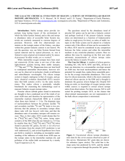
FIG. 1. a-Diagram of experimental setup: !-measuring electrode;
2-sample; 3-screen; R = I 00 ohm-input resistance of OK-33 oscilloscope. The arrows show the direction of propagation of the SW front.
b-equivalent circuit for the estimate of the thermal emf: 2) 2')-compressed (uncompressed) part of the sample; 3) 3 ')-compressed (uncompressed) part of the screen-cable-electrode system. I, III-sections of
the sample, 11-section formed by the SW front.
phase transition connected with the transition from a
semiconducting state into the metallic state. Therefore
at p = 20 or 40 kbar there propagates through the
sample a single elastic wave with velocity D = 8.5
km/ sec, and at p = 200 kbar there propagates a configuration of three compression waves (elastic wave,
first plastic SW, second plastic SW), the amplitudes of
which amount to 40, 72, and 128 kbar, respectively.
We subjected to shock loading samples of silicon
doped with boron (Si of p-type) and phosphorous
(n-type). Data on the specific volume resistance of the
sample p 0 and the impurity contents in them N are
given in Table 1. According to Pearson and Bardeen(sJ,
N corresponds approximately to the number of carriers. The sample length was l ~ 0.1-1 em and the
diameter ~2-3 em. A layer of aluminum 2-3 1J. thick
was deposited on the end surfaces. The sample surface
adjacent to the screen 3 was completely coated with
aluminum. The opposite end of the sample was covered
with aluminum only under the measuring electrode
(area S = 1 cm 2 ).
In the experiments we registered the time-varying
voltage drop U( t) across the input resistor R of the
oscilloscope. Since R » p 0 l/S, it follows that U(t) is
equal to the emf produced in shock-compressed samples. Typical U(t) oscillograms are shown in Fig. 2.
The experimental results have shown that the voltage
across R is produced at the instant when the SW enters
the sample (t = 0). The instant of emergence of the
elastic wave from the sample (T = Z/D) corresponds
in all cases to a drop in the voltage U( t). In comparing the experimental results it is best to use the
EXPERIMENT
1. The experimental setup is shown in Fig. 1a. The
samples were compressed by a plane SW perpendicular
to the (111) plane. The geometry of the explosive devices and the dimensions of the samples were such that
the attenuation of the SW and the influence of the
lateral relaxation in the sample could be neglected.
The measuring electrode (see 1 of Fig. 1a) was a
cadmium disc, whose acoustic stiffness was close to
that of silicon. This prevented reflection of the SW
from the electrode. The parameters of the SW in the
samples were calculated from the known state of the
screen (aluminum, copper) and the dynamic adiabat of
silicon[ 4 l. The experiments were performed at pressures (p) of 20, 40, and 200 kbar. It is known that the
Hugoniot elastic limit of silicon along the (111) axis is
40 kbar, and that at p = 112 kbar silicon experiences a
592
ELECTRIC SIGNALS IN SHOCK COMPRESSION OF DOPED SILICON
593
Table I. Volume resistivity and number of impurity atoms
in the initial samples. Experimental ( P 0 ) and calculated
(P) values of the polarization, electric field intensity, and
thickness of double layer in shock-compressed samples at
40 kbar pressure
Si
2.10-2
p-type {
n-type {
4,5
7,5
3,5.11)4
4,5
7,5
45
6.10"
1.10"*
7.1015
5·1011
2 .fOI>
9·10"
1·10"
2.1o-,
5.10-'
7 .1o-•
4.10-•
6.1c-•
-3.10-•
1.10-n - (2 ·10-" +2 .10-10) **
2.1Q-•
-5·10-S
3.1o-•
-5·10-•
4.10-10
-1.10-•
2 .1Q-8
4·10-•
fi.f0--<1
3·10-•
4.1Q-6
fi.f0-6
4.1o-s
2·10 7
4·10'
3-11}4
2
5.10•
5·104
3·10'
*In accordance with [5 ), the value of N given in ['] should be regarded as too low by
about' one order of magnitude.
**The first value corresponds to the condition 8 0 < t 0 , the second to 8 0 ~ t 0 . The
actual value ofP 0 therefore lies in the indicated range.
8
0
a
b
FIG. 3. Dependence of U 0 on the pressure at the SW front for p-Si
(a) and n-Si (b) at the following values of p: X-0.02; 0-4.5; 0-7.5;
6-3.5·10 4 ; e-45 ohm-em.
FIG. 2. Characteristic oscillograms of the voltages U(t) for Si: 1-5p-type, 6-8-n-type, 1-3 and 6-U= 0.15 V;4, 5, and 7, 8-U= 1.5 V.
The oscillograms were obtained in experiments with p equal to 20 kbar
(1), 40 kbar (2, 3, and 6), and 200 kbar (4, 5, and 7, 8). p 0 (in ohm-em)
and l (in em) are respectively: 1-0.02 and 0.28; 2-4.5, 0.38; 3-7.5;
0.3; 4-4.5; 0.49; 5-3.5 X 10⁴, 0.48; 6-4.5, 0.29; 7-4.5, 0.26; 8-7.5,
0.98. The arrows show the instants of entrance and emergence of SW
from the samples. The sweep is from left to right. Time markers-0.1
j.lsec.
quantity U0 (the value of U(t) extrapolated to t = 0 1 >
inasmuch as the initial part of the U(t) plot (the region
of the transients with characteristic time t 0 ~ 10- 9
sec) could not be resolved by the apparatus, and was
possibly distorted also by the fact that the SW did not
1 >For most plots of U(t), the value of U 0 obtained by extrapolation
does not exceed 30% of the experimentally registered values. However,
in cases similar to those shown, for example, in oscillograms 2 and 3 of
Fig. 2, the extrapolated value may differ from the experimental one by
a factor of 2.
enter the sample all at once. In a number of experiments, the front of the signal U(t) extended over a
time on the order of T and the plot of U(t) is a curve
with saturation (Fig. 2, 8). In this case U0 is taken to
be the value of U(t) in the saturation region. This
case will be discussed separately below.
2. The results of experiments on p-Si are shown in
Fig. 3a (see oscillograms 1 and 5 of Fig. 2), where
plots of U0 against p are given for samples with different p 0 • Each point on the plot is a result of a
separate explosion experiment. An analysis of the
experimental data has shown that, unlike the polarization of signals obtained with dielectrics [2 ' 3 \ the character of the U(t) plots and the value of U0 do not
depend on l (0.2-1 em), S (1-7 cm 2 ), orR (93-1053
ohm).
3. The results of the experiments on n-Si are shown
in Fig. 3b (see also oscillograms 6 and 8 of Fig. 2).
The data in Fig. 3 demonstrate the complicated character of the dependence of Uo on the type of the carriers, the number of impurity atoms, and the pressure
on the SW front in the investigated samples.
Let us note the following peculiarities in the plots
of U(t) for both types of silicon:
a) All the plots of U(t) can be approximated either
by the formula U ~ exp ( -t/ r) or by U ~ 1 -exp( -t/1) )2 )
(where r and 1J are certain time constants), or else
U = const. The dependence of the form of the registered signal on the parameters of shock-compressed
samples is illustrated by Table II.
2 >An exponential growth of U(t) was first observed by Novitski!
et al. in an investigation of polystyrene [ 6 ].
~
I
594
V. N. MINEER, et al.
Table II. Dependence of the registered signal on the
parameters of shock-compressed samples
Formula for U (t)
I
I
Si n-Si
p0 ,
ohm-em
;,
U .- e-1/t
U -1-e-'1"
U
=
const
{
{
;;
45
4.5: ~5; 45
Si p-Si
fp, kbar ot~:cffi"' I
i'~o"'
I
20
2~
4.5
2.1Q-2
:o; 40
:o; 40; zoo
7.5
3.5.10'
4.5
40; ~00
200
40; ,00
b) Not only U0 but also U ( t) is independent of T
when p = const. For example, for n-Si (p 0 = 4.5
ohm-em, p = 200 kbar) at values of T equal to 0.19,
0.3, 0.61, and 1.1 JJ.Sec, each succeeding plot of U(t)
duplicates the corresponding parts of the preceding
plots.
c) At p = 200 kbar, U( t) decreases when t > T to
the resolution limit of the measuring apparatus within
times on the order of 0.05-0.2 JJ.Sec. At all other
pressures, when t > T, the current in the measuring
circuit decreases to zero within a time ~o.2-0.5 JJ.Sec.
d) For plots in the form U ~ exp ( -t/T) with
t > T, the current in the circuit is opposite in direction to the current at t < T. In all other cases the
directions of the currents in the measuring circuit at
t > T and t < T coincide (see Fig. 2).
DISCUSSION
1. It is clear from general physical considerations
that the nature of the cons ide red effect is connected
either with volume or with surface phenomena occurring upon shock compression of semiconductors. We
shall show that the latter group of phenomena cannot
lead to the experimentally observed values of the emf.
To this end we turn to Fig. 1b and estimate the temperatures in the characteristic cross sections of the
sample.
A feature of the sections III (at t > 0) and I (at
t > T) is that in these sections there is produced a
contact between two shock-compressed substances
heated to different temperatures [7 1. In the course of
time, there is established in these sections a temperature
To= T'+kT'
z
t
k+ 1
T,
,
(A., c, and o are the thermal conductivity, the specific
heat per unit volume, and the density of the substances
in contact; the parameters with index 2 pertain to the
hotter substance). The dimension of the region v with
stationary temperature increases like v = ..; 4xt, where
x is the thermal-conductivity coefficient, equal to
~ 1 em 2/ sec (copper) and 10-2 cm 2/ sec (silicon) under
normal conditions. Within times t 0 ~ 10-9 sec (the
resolution time of the apparatus), v ~ 10-4-10-5 em.
An estimate shows that at p = 40 kbar we have TIII
= 318 and TI = 326°K. The calculation was carried out
under the assumption that the ratio of the values of c
and A. of shock-compressed silicon and copper (Sec.
lll), and also of silicon and cadmium (Sec. I) is the
same as under normal conditions. The temperature of
the shock-compressed silicon was determined from the
JJ.sec
I
p, kbar
1), j.Lsec
I
} 0.2-0.4
~0.1
} 0.1-1
relation T1f = Tg ( o/ o0), where o and o0 are the
densities of the silicon ahead of and behind the elasticwave front and y is the Gruneisen constant, equal to
0.43[ 8 1. At p = 40 kbar we have T1f = 275°K (Tg
273°K).
The calculated value of the temf at .a. T 0 = 35°, with
allowance for the static dependence of the Seebeck effect on the pressure (assumed to be the same as for
GaAsr 9 l, a semiconductor similar in its thermoelectric
properties to silicon) was 35 mV, which is smaller by
one order of magnitude than the experimentally
registered emf values. Another experimental fact that
cannot be attributed to the influence of surface effects
is that a current flows in the measuring circuit at
t > T, when .a. T 0 = 8°. One more fact confirming the
volume character of the observed emf is the independence of the sign of the emf in the investigated range of
p of the sign of the carriers (for example n-Si and
p-Si with N = 9 x 10 14 and N = 7 x 10 15 cm- 3 , respectively). This fact cannot be attributed to the reversal
of the sign of the carriers in the silicon upon shock
compression, as was the case in Kennedy's experimentsr10l, where it was shown that the reversal of the
sign of the carriers in n-Si ( p = 35 kbar) takes place
only at N s 7.5 x 10 13 cm- 3 • Finally, the assumption
that the effect has a thermoelectric nature is contradicted also by the following estimate. If the data of the
plots of Figs. 3a and 3b are represented in the form of
the functions a
U0/ .a. T 0 = f( ln N) at constant p, then
the linear sections of these relations have slopes from
86 to 1300 JJ.V/deg. According to semiconductor
theory[!!], on the other hand, the maximum slope of the
a = f( ln N) curves does not depend on the scattering
mechanism, the degree of degeneracy, or the electronic effective mass, and cannot exceed 86 1J. V/deg.
Thus, the presented facts indicate that the nature of
the observed emf is not connected with surface phenomena and consequently is due to a volume redistribution
of the charges, occurring following the shock compression of the investigated semiconductors (shock polarization).
2. Let us calculate the volume density of the bound
charges P(t). In differential form, the connection between the shock polarization P(t) and the parameters
of the measuring circuit and of the investigated substance, for an active load R, is written in the form[ 12 l
=
P(t)=)(Tt,F"(t)+[)(r(~, + ~
+[-)(T
u
where
K
+1)-()(-1)t]F'(t)
(~+1
+(~-~)t-()(-t)]F(t),
El,
El,
El
= w/10 0; 10 0 and
10
are the dielectric con-
(1)
ELECTRIC SIGNALS IN SHOCK COMPRESSION OF DOPED SILICON
stants of the substance in front of and behind the shock
wave; a = 6/6 0 ; t 0 = RC 0 is the relaxation time of the
measuring circuit, Co= £ 0 /41fl (S = 1 cm 2), ®0
= Po£o/41f, ® = p£/41f, p 0 , p-volume resistivities of
the matter in front of and behind the SW;
=
exp
t'
(-e,) Jj(t')exp ( 8 ) dt'
(
F(t)
I
I o
is the density of the charges on the measuring electrode and j( t) = U ( t )/ R is the density of the polar ization current.
In our experiments T ~ 10-6 sec, t 0 ~ 10-9 sec, and
®0 ~ 10-8-10- 14 sec. For semiconductors compressed
by weak SW we have p ~ p 0 [ 13l. Let us assume that in
the range of pressures under consideration we have
€ ~ £ 0 • In this case H ~ 1 and®~ ®0 •
Let us consider the case when
Ei ~ 8,,
x ~ 1;®,<to<T.
(2)
These conditions are satisfied for all the investigated
samples with the exception of p-Si with p 0 = 3.5
x 10 4 ohm-em. Taking (2) into account, Eq. (1) takes
the form
1
F"(t}+ (
1 )
1
P(t)
-+e, e F'(t)+-F(t)=-T-.
e,e
x t,
Let us compare
tained equation.
creases in such
increment of F
(3)
the terms in the left side of the obAssuming that the function F(t) ina way that after a time t ~ T the
is of the order of F itself, we obtain
F"(t)
~F/T',
F'(t)
~F/T.
Then, taking (2) into account, Eq. (3) at t
the form
xTt,
--j(t)=P(t).
(i,
e 0 takes
(5)
This means that for substances with good conductivity
on both sides of the SW front, unlike dielectrics, P(t)
can be readily obtained from j(t). Thus, in spite of the
fact that the thickness of the double layer is small
(A~ ® 0 D, see Table 1), nonetheless j(t) contains information concerning the processes of mechanical depolarization behind the SW frontl 14 l. In the particular
case when the polarization is established jumpwise and
a double layer propagates behind the shock-wave front
(T
T or ®
T), formula (5) coincides with that
previously obtained inl 1l.
«
«
Although the solution (5) is valid only for t » ® 0 ,
nonetheless it makes it possible to estimate the value
of P(t) close to t = 0, since ® 0 « T. If it is assumed
that there is a polarization jump on the SW front, then,
unlike in dielectrics, where Po = j 0 KT, in substances
with good conductivity, other conditions being equal,
the value of j 0 turns out to be smaller by a factor
t 0 /® 0 • In terms of the equivalent electric circuit, the
appearance of the factor t 0 / ® 0 = R/ p 0 l can be interpreted as the shunting influence of the resistance of
the investigated sample.
For t > T we assume in analogy with (2) that ®0
« t 0 « t - T. Then, taking (4) into account, we obtain
from (29) ofl 121
xTt,
--jp(t) = P{t)- P(t- T),
e,
where h(t) is the relaxation currentll 4• 15 J. Subtracting (5) from (6 ), we find that after a time t - T ~ t 0
we have
xTt,
-M=-P(t,),
(7 )
e,
where Aj = jr( T) - j( T). Thus, if the polarization on
the SW front reaches its maximum value within a time
t < t 0 , then a jump of the current will be observed at
t = T, in accordance with (7).
Inasmuch as the coefficient in (5) KTt 0 / ®0
= KR/ paD, it follows that j( t) is independent of the
sample thickness. This conclusion is confirmed by
experiment.
We shall show that the current i(t) in the circuit
does not depend on S. Indeed, since the emf in the
circuit of the polarization pickup does not depend on
the load, and the circuit resistance consists of R and
the sample resistance, we get
(R+
~~)it(tf=(R+ ~~)i,(t),
where i 1(t) and i 2(t) are the polarization currents in
samples with areas S1 and S2. At ® 0 « t 0 or pl/Sl
« R and pl/S 2 « R we have i 1(t) = i 2(t). In the case
of dielectrics, when pl/S » R, we get i 1(t)/S 1
=i2(t)/S2, i.e., i(t) = j(t)Sl 16 l.
The greater part of the obtained experimental data,
with account taken of (5), can be described by a single
formula
(8)
(4)
»
(6)
595
The physical meaning of (8) is that it represents in the
general case the process of establishment of polarization and mechanical depolarization in a shock-compressed substance. The term with exp ( -t/r) is the
consequence of the physically plausible assumption
that the process of mechanical depolarization per unit
volume of the medium is determined by the time that
this volume remains behind the SW frontl 17 J. The
second term represents the polarization-establishment
process connected, for example, with the finite region
of the real shock transition. As a first approximation,
the time dependence of this process is taken in the
form of an exponentially growing function, which describes qualitatively the experimentally obtained plot
of U(t) with a stretched out signal-establishment
front. We note that whereas at p = 200 kbar the value
1JD is comparable with the region of the phase transformation, at p = 40 kbar the quantity 1JD is apparently
much larger than the width of the shock transition.
The function (8) has a maximum at
t, = TJ In (1
(
+ ·t/TJ},
(9)
't ) -{H•I•) 't
P(t,)=P, 1+--;j
(10)
differentiating (5) and taking (8) into account, we obtain
p,JJ ( dj )-'
TJ =P,-.
xR dt. ,~,,
"";]"
(11)
If tM < T, then expressions (9)-(11) make it possible
to find Po, T, and 1J. In the particular case when
T » T or 1J- 0, Eq. (8) simplifies to
(12)
or
(13)
V. N. MINEEV, et al.
596
-ro~--------~----~f--------------~z
t/T
FIG. 4. Values of(T/17) and (T/r) for the theoretical curves: 1-1(1);
2-1(0); 3-1 0(0); 4-0.1(0); 5-oo(l ); 6-oo (I 0); 7-oo (0.1).
Table III
Si
Po. ohm-em
P 0 , C-cm· 2
4.5
1,6-10-'
fl, Jl.sec
1'.97
n~i
7.5
1.1·10-'
0. 75
Si p-si
45
8-11.-S
7.5
10-'
0.55
11.1
The values of Po and 11 can be determined from (11)
and (12), and P 0 and T can be found from (13) at t =to
and t = T. The value of T can also be obtained from
the polarization jump at t = T:
..: =
T {In (1- jp(T) !i(T) ]}-'.
The curves of the polarization current ( 0 < t < T)
and of the relaxation current ( T < t < 2T) calculated
from (5) and (6), with account taken of (8), for different
values of T and 1], are shown in Fig. 4. A comparison
of the calculated and the experimental U(t) curves
shows a qualitative agreement between experiment and
calculation. The values of P 0 = f( N) calculated from
(5) at p = 40 kbar are given in Table I. The values of
P 0 and 11 at p = 200 kbar, for different values of p 0 ,
determined from (11) and (12), are listed in Table III.
3. The mechanism of the shock polarization of silicon is not clear in many respects. However, the large
values of T and 11 obtained from the reduction of the
experimental data, and also the fact that P 0 increases
with N, offer evidence in favor of the hypothesis advanced by us earlier[ 1 ' 2 l, namely the volume redistribution of the ionized impurity atoms during the course
of the passage of the shock wave through the silicon.
It can be assumed further that as a result of the
smaller dimensions of the impurity ions (the radius of
the boron anion is 0.89 A and that of the phosphorus
cation is 1.1 A), compared with the silicon atoms
(1.17 A[sJ) and the low binding energy of the impurities
with the main lattice (0.044 eV[ 181 ), the mechanism of
volume polarization consists in the following: 1) formation of bound or separated Frenkel pairs possessing an
electric moment by the impurities under the influence
of the shock wave, and 2) orientation of these pairs in
the direction of motion of the shock wave. This assumption is confirmed by the data of[ 19 1, where it is
shown that with increasing degree of doping of the
silicon the number of point defects produced after
shock loading increases.
The electric field produced upon polarization becomes cancelled out after a time ® by the field of the
carriers. This state of matter is analogous to the
state of the "short circuited" electret, in which the
total field is equal to zero at nonzero polarization [201.
However, whereas the electret can remain in such a
state for a sufficiently long time, in the case of a shockcompressed semiconductor this time may be comparable with the characteristic time of the experiment (T).
The process of establishment of the thermodynamic
equilibrium will be characterized by a time T and can
consist in the fact that during the time ~ T the ions of
the impurities occupy the vacancies. This depolarization process will cause a change in the electric field of
the carriers. If T ~ ®, then the law governing the
variation of this field with time will coincide with the
law governing the change of polarization.
Let us estimate the order of magnitude of the
polarization of silicon within the framework of the
hypothesis under consideration. We assume that all
the ionized atoms of the impurity are displaced by one
lattice period along the direction of propagation of the
shock wave relative to the lattice of the host material.
Then the polarization of 1 em 3 of matter is P = qN 213 ,
where N is the number of ionized impurity atoms with
charge q equal to the electron charge. The results of
the calculation are listed in Table 1. Comparisons of
the values of P obtained from the foregoing estimate
and from the reduction of the experimental data with
the aid of the phenomenological theory (see Table I)
show these quantities to be in qualitative agreement.
From the fact that P 0 depends on N and p it
follows that the direction of the displacement of the
impurity ions in the SW front relative to the lattice
of the silicon itself is a function of N and p. Thus,
for example, it must be assumed that at p = 200 kbar
the phosphorus cations move against the direction of
propagation of the shock wave, and the boron anions in
its direction (independently of the number N). At
p = 40 kbar and Po= 4.5 ohm-em, the displacement of
the phosphorus and boron ions in the SW front is in the
direction of the SW propagation.
The presence of shock polarization in a substance
with good conductivity ahead of and behind the SW
front means that a double electric layer of thickness
A = ®D propagates in such a medium together with the
front (at 11 = 0 ). Assuming that the potential difference
across this layer is equal to the value of U0 observed
in the experiment, let us estimate the field intensity E
in this layer: E 2: U0 / A. The obtained values of A and
E for the investigated samples at p = 40 kbar are
listed in Table I.
We note that the conclusions of the phenomenological theory of shock polarization, drawn in the present
paper, can apparently be extended also to substances
with better conductivity than the investigated semiconductors. We note in this connection that an emf of the
order of 10-100 mV was observed by the authors in
shock compression of a number of metals (bismuth[ 21 l,
beryllium, zinc, magnesium, ytterbium) at
p = 100-1000 kbar. It is possible that it is precisely
the shock polarization of the metals which explains the
results of a number of authors[ 22 ' 23 ' 7 l who investigated
the emf of the shock-compressed pair nickel-copper.
In the cited papers, the observed emf ( ~ 10-30 mV)
turned out to be 2-4 times larger than the expected
emf.
ELECTRIC SIGNALS IN SHOCK COMPRESSION OF DOPED SILICON
In the case of U(t) = const, one cannot exclude the
possibility that the observed emf is due to volume
processes with short transient times, for example with
electronic polarization. Let us estimate the maximum
value of the emf behind the SW front due to electronic
polarization of the medium, from the condition that the
field intensity E in the double layer does not exceed
the breakdown values. Putting E ~ 10 6 V, we find
U ~ E ;D ~ 5 mV, where ; ~ 10- 14 sec is the relaxation
time of the electronic polarization. An emf of this
order of magnitude cannot be discerned in shock compression of dielectrics (in view of the tremendous
internal resistance possessed by the dielectric when
regarded as the source of the emf), but can be measured in the case of motion of a shock wave through
semiconductors or metals.
We note that we found no acceptable explanation for
the following facts:
a) The emergence of the elastic wave at the measuring electrode (t = T) is accompanied in all cases by
a decrease of U( t). This means that P( t) should also
be determined only by the parameters of the elastic
wave, i.e., U(t) should be independent of the pressure
in the pressure interval from 40 to 200 kbar. This,
however, is not confirmed by the experiment.
b) As indicated above, the change of p from 40 to
200 kbar leads to a radical difference in the structure
of the SW front. However, in view of the insufficiency
of the experimental data, it is impossible to estimate
the contribution made to P(t) by each of the three
waves at p = 200 kbar.
CONCLUSIONS
1. The emf observed following shock compression
of silicon is due principally to volume processes behind the SW front, i.e., to shock polarization. The dependence of the surface density of the bound charges on
the SW front on the number of impurity atoms, and also
the large times of establishment and destruction of the
polarization, indicate that the mechanism of the phenomenon is apparently connected with the ionized impurity atoms.
2. Unlike in dielectrics, the polarization current recorded in the external circuit following shock compression of semiconductors is determined only by the timevarying polarization.
3. The thermodynamic equilibrium in the electric
phenomena under consideration is characterized by the
relaxation times 'T ~ 0.1-1 JJ.Sec. Times of the same
order are characteristic of shock-polarization processes in ionic crystals [l4J and in organic substances
consisting of polar molecules (see, for example,P 51 ).
This indicates the absence of a strictly thermodynamic
equilibrium behind the SW front in the substances under consideration 3 >. However, the noted effect is small,
since the change of the external energy of these substances due to the shock polarization amounts to
10-7 -10- 3 % of its total increment on the SW front
( ~ 10 10 erg/ em 3 ).
3l A similar conclusion was drawn by Luzin [ 24 ] on the basis of a
theoretical analysis of the motion of shock waves in an ideal crystal
lattice.
597
A further study of the mechanism of shock polarization of semiconductors is expected to be connected with
investigations of the phenomenon of the growth of
polarization behind the shock front, with clarification
of the roles of elastic and plastic waves in the polarization of silicon, and also with physical interpretation
of the reversal of the sign of the polarization with
changing pressure on the SW front.
1 V. N. Mineev, A. G. Ivanov, E. Z. Novitskil, Yu.
N. Tyunayaev and Yu. V. Lisitsyn, ZhETF Pis. Red. 5,
296 (1967) [JETP Lett. 5, 244 (1967)).
2 V. N. Mineev, Yu. N. Tyunyaev, A. G. Ivanov, E. Z.
Novitskit, and Yu. V. Lisitsyn, Zh. Eksp. Teor. Fiz.
53, 1242 (1967) [Sov. Phys.-JETP·26, 728 (1968)].
3 A. N. Dremin, 0. K. Rozanov, and V. V. Yakushev,
Prik. Mat. Teor. Fiz. 5, 53 (1968).
4 M, N. Pavlovskit, Fiz. Tverd. Tela 9, 3192 (1967)
[Sov. Phys.-Solid State, 9, 2514 (196 )].
5 G. L. Pearson and J. Bardeen, Phys. Rev., 7 5, 865
(1949).
6 E. z. Novitskil, V. N. Mineev, A. G. Ivanov, E. S.
Tyun'kin, z. I. Peshkova, N. P. Khokhlov, and F. I.
Tsyplenkov, Polarization Properties of Organic Substances in Shock Waves, Avtoreferaty dokladov na
Vtorom Vsesoyuznom simpoziume po goreniyu i
vzryvu, (Abstracts of Papers at 2nd Symp. on Combustion and Explosion), Erevan, October 1969, p. 269.
7 0. I. Buzhinski'l and S. V. Samylov, Fiz. Tverd.
Tela, 11, 2881 (1969) [Sov. Phys.-Solid State, 11, 2332
(1970)].
8 D. F. Gibbons, Phys. Rev. 112, 136 (1958).
9 Solids Under Pressure, ed. W. Paul, D. M.
Warshauer, McGraw-Hill Book Comp., 1963. p. 261.
10 J. Kennedy, Hall Effects Measurements in ShockLoaded Semiconductors, Symposium High Dynamic
Pressure, Paris 11-15 Sept. 1967.
11 L. s. Stil'bans, Fizika poluprovodnikov (Physics of
Semiconductors) Sov. Radio 1967.
12 R. M. Zaidel', Zh. Eksp. Teor. Fiz. 54, 1253
(1968) [Sov. Phys.-JETP 27, 670 (1968)].
13 R, A. Graham, 0. E. Jones, and J. R. Holland,
J. Phys. Chern. Solids, 27, 1519 (1966).
14 A. G. Ivanov, E. Z. Novitski!, V. N. Mineev, Yu.
V. Lisitsin, Yu. N. Tyunyaev and G. I. Bezrukov, Zh.
Eksp. Teor. Fiz. 53, 41 (1967) [Sov. Phys.-JETP 26,
28 (1968)].
15 V. V. Yakushev, 0. K. Rozanov, and A. N. Dremin,
Zh. Eksp. Teor. Fiz. 54, 396 (1968) (Sov. Phys.-JETP
27' 213 (1968)].
16 R. J. Eichelberger and G. E. Hauver, Les ondes
de detonation, Paris, 1961, p. 364.
17 F, E. Allison, J. Appl. Phys. 36, 2111, 1965.
18 C. A. Wert, R. M. Thomson, Physics of Solids,
McGraw-Hill Book Comp., N. Y.-L, 1964, p. 323.
19 N. A. Meshcheryakov and T. A, Sharapova, Izv.
Sibirskogo otd. AN SSSR, seriya khim. nauk (Bull.
Siberian Div. Acad. Sci. USSR, Chern. Series) No.9
(129), 4, 60, 1967._
20 A. N. Gubkin, Elektrety (Electrets) AN SSSR, 1961.
21 A. G. Ivanov, V. N. Mineev, E. z. Novitski!:, Yu.
598
V. N. MINEEV, et al.
V. Lisitsyn, and Yu. N. Tyunyaev, ZhETF Pis. Red. 7,
191 (1968) (JETP Lett. 7, 147 (1968)].
22 J. Jacquesson, Bull. G.A.M.A., 4, 33, 1959.
23 V" C. llyuhin and V. N. Kologrivov, Prikl. Mat.
Teor. Fiz. 5,176 (1962).
24 A. N. Luzin, Possible Absence of Thermodynamic
Equilibrium behind the Front of a Shock Wave in a
Crystal, Avtoreferaty dokladov na Vtorom Vsesoyuznom
simpoziume po goreniyu i vzryvu, (Abstracts of Papers
at 2nd All-union Symp. on Combustion and Explosion)
Erevan, October 1969, p. 278.
Translated by J. G. Adashko
126
© Copyright 2026 ExpyDoc