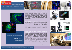
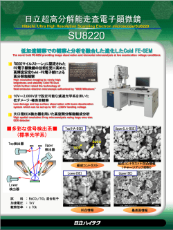
Mission
The mission of the Connecticut State Colleges &
Universities (ConnSCU) Center for Nanotechnology
is to foster collaborative, interdisciplinary research
and educational initiatives/programs in micro- and
nanotechnology with the goal of enhancing
Connecticut’s workforce competitiveness in
nanotechnology and materials science. The Center
builds upon existing collaborations with Yale
University, The University of Connecticut and the
Connecticut Community Colleges to create programs
enhancing Science, Technology, Engineering, and
Mathematics (STEM) education for the ConnSCU
community and beyond. The ConnSCU Center for
Nanotechnology is the primary resource for SCSU’s
Nanotechnology Graduate Certificate, the Applied
Physics Masters: Nanotechnology/Materials Science
track, as well as an array of research opportunities
and professional development for students and
faculty. Center instrumentation and programs are
partially funded by grants from the National Science
Foundation [NSF] and the Department of Energy
[DOE].
Our Equipment
Equipment in the NanoCenter supports synthesis,
processing, and characterization of micro- and nanoscale materials. Synthesis options include wet
chemical methods for thin films and nanoparticles
(quantum dots), and chemical vapor deposition
systems for carbon nanotube (CNT) growth and thin
film deposition. Transmission Electron Microscopy
(TEM) sample preparation is well supported with
options for polishing, milling, and slicing samples.
Nanocharacterization is a strength at SCSU that is
built around the data acquisition and analysis from
an array of transmission, scanning electron, and
force microscopy instruments. The NanoCenter is
active in efforts to expand its equipment and
expertise capabilities.
For more information:
Dr. Christine Broadbridge
Director, ConnSCU-CNT
(203) 392-6461
[email protected]
Dr. Matthew Enjalran
(203) 3925444
[email protected]
Dr. Todd Schwendemann
(203) 392-6431
[email protected]
501 Crescent Street
New Haven, CT 06515
SouthernCT.edu
Scanning Electron
Microscopy
Ion Mill
Zeiss Sigma VP
This is a field emission SEM
capable of spatial resolutions of
1.5 nm. This is a variable
pressure system allowing for
examination of insulating
samples without addition of
conducting coatings. The
system contains In-lens SE,
Everhart-Thornley, Backscatter
and EDS detectors.
Transmission Electron
Microscopy
Phillips EM400
120kV TEM capable of resolving
down to 0.3 nm; the system is
heavily used in nano-scale
investigations of interfaces and
thin films. An Oxford EDX
attachment is added allowing
high spatial resolution
elemental analysis.
Scanning Electron Microscope
(tabletop)
Hitachi TM1000
The system is a portable SEM with a
10,000 X magnification. Ideally
suited for looking at a wide variety
of small samples. It also contains an
EDS detector allowing elemental
composition.
Dip Pen Nanolithography (DPN)
Nanoink NLP-2000
Nanolithography instrument capable
of depositing a wide variety of
materials with sub-micron accuracy
and precision. Used for multiplexed
protein printing, biosensor
functionalization, nanopattering
studies, polymer pattering.
Optical Microscope
Gentle Mill TL-GM1
Low Energy Argon Ion
bombardment beam
instrument designed for
preparing TEM samples to
thicknesses < 100 nm.
Olympus BH2
Optical Microscopes
Zeiss Axio Lab A1
and
Zeiss Axio Scope A1
Ultra-Microtome
Sorvall Porter Ultramicrotome MT-2
Used for sectioning of polymer or
biologic samples with thickness
between 50 nm - 100 microns.
Chemical Vapor Deposition
Carbon Nanotube Synthesis
Nanotech Innovations SSP-354
Growth of multi-wall carbon
nanotubes using a nanoparticle
catalysis infused liquid
precursor.
TEM Prep
Allied High Tech 15-2000 GI
MultiPrep
The MultiPrep enables precise
semi-automatic sample
preparation
Precision Low Speed
Diamond Saw
UV-Vis-NIR
Shimadzu UV-3600
Contains three detectors and
high performance double
monochromator. Used for
ensemble average quantum
dot-size measurements.
Allied High Tech
A low speed saw excellent for
cutting small delicate samples.
Cutting of crystals and very
hard materials with precision is
also possible.
Inverted Optical Microscope
Olympus Gx71
An inverted optical microscope
for metallurgical images.
Scanning Probe Microscope (AFM and STM)
Vecco Multimode Rev 8 Nanonis RT control
electronics
Atomically sharp tips raster across a sample
surface generating topography map with atomic
scale detail. The multimode SPM can examine
conductive as well as non-conductive samples.
Additionally, biological samples can be
examined using a fluid cell attachment.
Additional Instrumentation is available to the
ConnSCU Nanotechnology Center with collaboration
from all Connecticut state universities.
SouthernCT.edu
Funding by NSF MRSEC DMR 1119826 • DOE DE-SC0005904 • DOE DESC0005072
© Copyright 2026 ExpyDoc