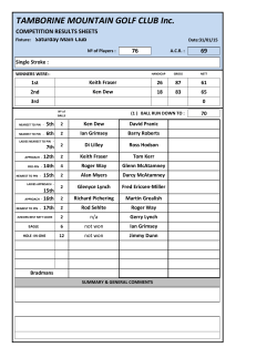
AVR IO Ports General Purpose I/Os, Pull-Up Resistors, Programming IOs Credit to Dr. Robucci for slide information ATMega169P Chip I/O Ports • All AVR Ports have true Read-Modify-Write functionality ▫ Each pin on a port can be modified without unintentionally modifying any other pin • Three I/O memory address locations allocated for each port ▫ Data Register – PORTx (Read/Write) ▫ Data Direction Register – DDRx (Read/Write) ▫ Port Input Pins – PINx (Read) I/O Ports • ATMega 169P has 7 ports ▫ A,B,C,D,E,F,G • Pxn represents nth bit in Port x ▫ E.g. PA6 == 6th bit of Port A • If DDxn is a: ▫ 1 – Pxn is configured to be an output pin ▫ 0 – Pxn is configured to be an input pin • If DDxn is configured as output and PORTxn is: ▫ 1 – Pxn is driven high (1) ▫ 0 – Pxn is driven low (0) • Note: “writing” a logic 1 to a bit in the PINx Register will toggle the corresponding bit in the data General Digital I/O Pull-Up Resistor S1 = 0 – High Impedance S1 = 1 – VCC BAD S1 = 0 – GND S1 = 1 – VCC BAD Why? S1 = 0 – GND S1 = 1 - VCC Good Why? Pull-Up Resistor • With a pull-up resistor, the input pin reads high state when switch is open, low when switch is closed • AVR has internal pull-up ▫ No need to implement outside • This is what allows you to toggle the pin’s output Programming I/O Ports - Assembly • • • • ;Using CBI and SBI to write to ports SBI DDRB, 1 ;make bit 1 as output bit on PORTB CBI PORTB, 1 ;make PORTB bit 1 as "0" SBI PORTB, 1 ;make PORTB bit 1 as "1" • • • • • • • ;Using OUT instruction to write to ports LDI R18, 0b00010000 OUT DDRB, R18 ;make bit 1 as output bit on PORTB LDI R18, 0b00000000 OUT PORTB, R18 ;make PORTB bit 1 as "0" LDI R18, 0b00010000 OUT PORTB, R18 ;make PORTB bit 1 as "1“ Programming I/O Ports - Assembly • • • • • • • ;INPUT EXAMPLE IN R18,PINB ;set pin 5 of B port as output ; without affecting other bits IN R18,DDRB ORI R18, 0b00010000 OUT DDRB, R18 • • • • • ;set pin 5 of B port to 1 ; without affecting other bits IN R18,PORTB ORI R18, 0b00100000 OUT PORTB, R18 Programming I/O Ports - Assembly • • • • • ;clear pin 5 of B port to 0 ; without affecting other bits IN R18,PORTB ANDI R18, 0b11101111 OUT PORTB, R18 • • • • • ;set pin 7,3 of B port to 1 at same time ; without affecting other bits IN R18,PORTB ORI R18, 0b10001000 OUT DDRB, R18 Programming I/O Ports - Assembly • • • • • • ;toggle pin 1 of B (no eori available) ; without affecting other bits IN R18,PORTB LDI R19,0b00000010 EOR R18, R19 OUT PORTB, R18 • ;toggle pin 1 of B using PINB "input write trick" • OUT PINB, 0b00000010 Ports on Butterfly Board Review of Bit masking • Controlling Port I/O makes bit masks invaluable ▫ Allows control of single pins without affecting others • Using OR as mask to bring up a pin ▫ ORI A 0’b0000001 Only makes the LSB become 1, leaves others unaffected • Using AND as mask to bring a pin down ▫ ANDI A 0’b1111110 Only makes LSB become 0, leaves others unaffected
© Copyright 2026 ExpyDoc