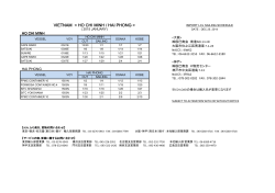
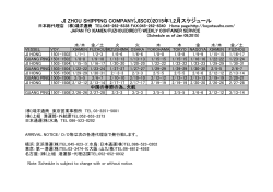
SST25VF080B 8 Mbit SPI Serial Flash Features • Single Voltage Read and Write Operations - 2.7-3.6V • Serial Interface Architecture - SPI Compatible: Mode 0 and Mode 3 • High Speed Clock Frequency - 50/66 MHz conditional (see Table 5-6) • Superior Reliability - Endurance: 100,000 Cycles (typical) - Greater than 100 years Data Retention • Low Power Consumption: - Active Read Current: 10 mA (typical) - Standby Current: 5 μA (typical) • Flexible Erase Capability - Uniform 4 KByte sectors - Uniform 32 KByte overlay blocks - Uniform 64 KByte overlay blocks • Fast Erase and Byte-Program: - Chip-Erase Time: 35 ms (typical) - Sector-/Block-Erase Time: 18 ms (typical) - Byte-Program Time: 7 μs (typical) • Auto Address Increment (AAI) Programming - Decrease total chip programming time over Byte-Program operations • End-of-Write Detection - Software polling the BUSY bit in Status Register - Busy Status readout on SO pin in AAI Mode • Hold Pin (HOLD#) - Suspends a serial sequence to the memory without deselecting the device • Write Protection (WP#) - Enables/Disables the Lock-Down function of the status register • Software Write Protection - Write protection through Block-Protection bits in status register • Temperature Range - Commercial: 0°C to +70°C - Industrial: -40°C to +85°C 2014 Microchip Technology Inc. • Packages Available - 8-lead SOIC (200 mils) - 8-contact WSON (6mm x 5mm) - 8-lead PDIP (300 mils) • All devices are RoHS compliant Product Description 25 series Serial Flash family features a four-wire, SPIcompatible interface that allows for a low pin-count package which occupies less board space and ultimately lowers total system costs. The SST25VF080B devices are enhanced with improved operating frequency and lower power consumption. SST25VF080B SPI serial flash memories are manufactured with proprietary, high-performance CMOS SuperFlash technology. The split-gate cell design and thick-oxide tunneling injector attain better reliability and manufacturability compared with alternate approaches. The SST25VF080B devices significantly improve performance and reliability, while lowering power consumption. The devices write (Program or Erase) with a single power supply of 2.7-3.6V for SST25VF080B. The total energy consumed is a function of the applied voltage, current, and time of application. Since for any given voltage range, the SuperFlash technology uses less current to program and has a shorter erase time, the total energy consumed during any Erase or Program operation is less than alternative flash memory technologies. The SST25VF080B device is offered in 8-lead SOIC (200 mils), 8-contact WSON (6mm x 5mm), and 8-lead PDIP (300 mils) packages. See Figure 2-1 for pin assignments. DS20005045B-page 1 SST25VF080B 1.0 BLOCK DIAGRAM FIGURE 1-1: FUNCTIONAL BLOCK DIAGRAM SuperFlash Memory X - Decoder Address Buffers and Latches Y - Decoder I/O Buffers and Data Latches Control Logic Serial Interface 1296 B1.0 CE# DS20005045B-page 2 SCK SI SO WP# HOLD# 2014 Microchip Technology Inc. SST25VF080B 2.0 PIN DESCRIPTION FIGURE 2-1: PIN ASSIGNMENTS CE# 1 SO 2 8 VDD 7 HOLD# CE# 1 SO 2 8 VDD 7 HOLD# Top View Top View WP# 3 6 SCK WP# 3 6 SCK VSS 4 5 SI VSS 4 5 SI 1296 08-soic S2A P1.0 1296 08-wson QA P2.0 8-lead SOIC 8-contact WSON CE# SO VDD Top View HOLD# WP# SCK VSS SI 1296 08-pdip-PA-P3.0 8-lead PDIP TABLE 2-1: PIN DESCRIPTION Symbol Pin Name Functions SCK Serial Clock To provide the timing of the serial interface. Commands, addresses, or input data are latched on the rising edge of the clock input, while output data is shifted out on the falling edge of the clock input. SI Serial Data Input To transfer commands, addresses, or data serially into the device. Inputs are latched on the rising edge of the serial clock. SO Serial Data Output To transfer data serially out of the device. Data is shifted out on the falling edge of the serial clock. Outputs Flash busy status during AAI Programming when reconfigured as RY/BY# pin. See “Hardware End-of-Write Detection” on page 10 for details. CE# Chip Enable The device is enabled by a high to low transition on CE#. CE# must remain low for the duration of any command sequence. WP# Write Protect The Write Protect (WP#) pin is used to enable/disable BPL bit in the status register. HOLD# Hold To temporarily stop serial communication with SPI flash memory without resetting the device. VDD Power Supply To provide power supply voltage: 2.7-3.6V for SST25VF080B VSS Ground 2014 Microchip Technology Inc. DS20005045B-page 3 SST25VF080B 3.0 used to select the device, and data is accessed through the Serial Data Input (SI), Serial Data Output (SO), and Serial Clock (SCK). MEMORY ORGANIZATION The SST25VF080B SuperFlash memory array is organized in uniform 4 KByte erasable sectors with 32 KByte overlay blocks and 64 KByte overlay erasable blocks. 4.0 The SST25VF080B supports both Mode 0 (0,0) and Mode 3 (1,1) of SPI bus operations. The difference between the two modes, as shown in Figure 4-1, is the state of the SCK signal when the bus master is in Stand-by mode and no data is being transferred. The SCK signal is low for Mode 0 and SCK signal is high for Mode 3. For both modes, the Serial Data In (SI) is sampled at the rising edge of the SCK clock signal and the Serial Data Output (SO) is driven after the falling edge of the SCK clock signal. DEVICE OPERATION The SST25VF080B is accessed through the SPI (Serial Peripheral Interface) bus compatible protocol. The SPI bus consist of four control lines; Chip Enable (CE#) is FIGURE 4-1: SPI PROTOCOL CE# SCK MODE 3 MODE 3 MODE 0 MODE 0 Bit 7 Bit 6 Bit 5 Bit 4 Bit 3 Bit 2 Bit 1 Bit 0 SI MSB HIGH IMPEDANCE DON T CARE Bit 7 Bit 6 Bit 5 Bit 4 Bit 3 Bit 2 Bit 1 Bit 0 SO MSB 4.1 Hold Operation The HOLD# pin is used to pause a serial sequence underway with the SPI flash memory without resetting the clocking sequence. To activate the HOLD# mode, CE# must be in active low state. The HOLD# mode begins when the SCK active low state coincides with the falling edge of the HOLD# signal. The HOLD mode ends when the HOLD# signal’s rising edge coincides with the SCK active low state. If the falling edge of the HOLD# signal does not coincide with the SCK active low state, then the device enters Hold mode when the SCK next reaches the active low state. Similarly, if the rising edge of the FIGURE 4-2: 1296 SPIprot.0 HOLD# signal does not coincide with the SCK active low state, then the device exits in Hold mode when the SCK next reaches the active low state. See Figure 4-2 for Hold Condition waveform. Once the device enters Hold mode, SO will be in highimpedance state while SI and SCK can be VIL or VIH. If CE# is driven active high during a Hold condition, it resets the internal logic of the device. As long as HOLD# signal is low, the memory remains in the Hold condition. To resume communication with the device, HOLD# must be driven active high, and CE# must be driven active low. See Figure 5-3 for Hold timing. HOLD CONDITION WAVEFORM SCK HOLD# Active Hold Active Hold Active 1296 HoldCond.0 DS20005045B-page 4 2014 Microchip Technology Inc. SST25VF080B 4.2 4.2.1 Write Protection The Write Protect (WP#) pin enables the lock-down function of the BPL bit (bit 7) in the status register. When WP# is driven low, the execution of the WriteStatus-Register (WRSR) instruction is determined by the value of the BPL bit (see Table 4-1). When WP# is high, the lock-down function of the BPL bit is disabled. SST25VF080B provides software Write protection. The Write Protect pin (WP#) enables or disables the lockdown function of the status register. The Block-Protection bits (BP3, BP2, BP1, BP0, and BPL) in the status register provide Write protection to the memory array and the status register. See Table 4-3 for the BlockProtection description. TABLE 4-1: 4.3 CONDITIONS TO EXECUTE WRITE-STATUS-REGISTER (WRSR) INSTRUCTION WP# BPL L 1 Not Allowed L 0 Allowed H X Allowed Execute WRSR Instruction Status Register The software status register provides status on whether the flash memory array is available for any Read or Write operation, whether the device is Write enabled, and the state of the Memory Write protection. TABLE 4-2: Bit 0 WEL 2 3 4 5 6 BP0 BP1 BP2 BP3 AAI 7 BPL 4.3.1 Function 1 = Internal Write operation is in progress 0 = No internal Write operation is in progress 1 = Device is memory Write enabled 0 = Device is not memory Write enabled Indicate current level of block write protection (See Table 4-3) Indicate current level of block write protection (See Table 4-3) Indicate current level of block write protection (See Table 4-3) Indicate current level of block write protection (See Table 4-3) Auto Address Increment Programming status 1 = AAI programming mode 0 = Byte-Program mode 1 = BP3, BP2, BP1, BP0 are read-only bits 0 = BP3, BP2, BP1, BP0 are read/writable BUSY The Busy bit determines whether there is an internal Erase or Program operation in progress. A “1” for the Busy bit indicates the device is busy with an operation in progress. A “0” indicates the device is ready for the next valid operation. 4.3.2 During an internal Erase or Program operation, the status register may be read only to determine the completion of an operation in progress. Table 4-2 describes the function of each bit in the software status register. SOFTWARE STATUS REGISTER Name BUSY 1 WRITE PROTECT PIN (WP#) WRITE ENABLE LATCH (WEL) The Write-Enable-Latch bit indicates the status of the internal memory Write Enable Latch. If the WriteEnable-Latch bit is set to “1”, it indicates the device is Write enabled. If the bit is set to “0” (reset), it indicates the device is not Write enabled and does not accept 2014 Microchip Technology Inc. Default at Power-up 0 Read/Write R 0 R 1 1 1 0 0 R/W R/W R/W R/W R 0 R/W any memory Write (Program/Erase) commands. The Write-Enable-Latch bit is automatically reset under the following conditions: • • • • • • • • Power-up Write-Disable (WRDI) instruction completion Byte-Program instruction completion Auto Address Increment (AAI) programming is completed or reached its highest unprotected memory address Sector-Erase instruction completion Block-Erase instruction completion Chip-Erase instruction completion Write-Status-Register instructions DS20005045B-page 5 SST25VF080B 4.3.3 AUTO ADDRESS INCREMENT (AAI) BP1 and BP0 bits as long as WP# is high or the BlockProtect-Lock (BPL) bit is 0. Chip-Erase can only be executed if Block-Protection bits are all 0. After powerup, BP3, BP2, BP1 and BP0 are set to 1. The Auto Address Increment Programming-Status bit provides status on whether the device is in AAI programming mode or Byte-Program mode. The default at power up is Byte-Program mode. 4.3.4 4.3.5 BLOCK PROTECTION (BP3,BP2, BP1, BP0) WP# pin driven low (VIL), enables the Block-ProtectionLock-Down (BPL) bit. When BPL is set to 1, it prevents any further alteration of the BPL, BP3, BP2, BP1, and BP0 bits. When the WP# pin is driven high (VIH), the BPL bit has no effect and its value is “Don’t Care”. After power-up, the BPL bit is reset to 0. The Block-Protection (BP3, BP2, BP1, BP0) bits define the size of the memory area, as defined in Table 4-3, to be software protected against any memory Write (Program or Erase) operation. The Write-Status-Register (WRSR) instruction is used to program the BP3, BP2, TABLE 4-3: BLOCK PROTECTION LOCK-DOWN (BPL) SOFTWARE STATUS REGISTER BLOCK PROTECTION FOR SST25VF080B1 Status Register Bit2 Protection Level Protected Memory Address BP3 BP2 BP1 BP0 8 Mbit X 0 0 0 None Upper 1/16 X 0 0 1 F0000H-FFFFFH Upper 1/8 X 0 1 0 E0000H-FFFFFH Upper 1/4 X 0 1 1 C0000H-FFFFFH Upper 1/2 X 1 0 0 80000H-FFFFFH All Blocks X 1 0 1 00000H-FFFFFH All Blocks X 1 1 0 00000H-FFFFFH All Blocks X 1 1 1 00000H-FFFFFH None 1. X = Don’t Care (RESERVED) default is “0 2. Default at power-up for BP2, BP1, and BP0 is ‘111’. (All Blocks Protected) DS20005045B-page 6 2014 Microchip Technology Inc. SST25VF080B 4.4 of CE#. Inputs will be accepted on the rising edge of SCK starting with the most significant bit. CE# must be driven low before an instruction is entered and must be driven high after the last bit of the instruction has been shifted in (except for Read, Read-ID, and Read-StatusRegister instructions). Any low to high transition on CE#, before receiving the last bit of an instruction bus cycle, will terminate the instruction in progress and return the device to standby mode. Instruction commands (Op Code), addresses, and data are all input from the most significant bit (MSB) first. Instructions Instructions are used to read, write (Erase and Program), and configure the SST25VF080B. The instruction bus cycles are 8 bits each for commands (Op Code), data, and addresses. Prior to executing any Byte-Program, Auto Address Increment (AAI) programming, Sector-Erase, Block-Erase, Write-Status-Register, or Chip-Erase instructions, the Write-Enable (WREN) instruction must be executed first. The complete list of instructions is provided in Table 4-4. All instructions are synchronized off a high to low transition TABLE 4-4: DEVICE OPERATION INSTRUCTIONS Instruction Description Op Code Cycle1 Address Cycle(s)2 Dummy Cycle(s) Data Cycle(s) Read Read Memory 0000 0011b (03H) 3 0 1 to High-Speed Read Read Memory at higher speed 0000 1011b (0BH) 3 1 1 to 4 KByte Sector-Erase3 Erase 4 KByte of memory array 0010 0000b (20H) 3 0 0 32 KByte Block-Erase4 Erase 32 KByte block of memory array 0101 0010b (52H) 3 0 0 64 KByte Block-Erase5 Erase 64 KByte block of memory array 1101 1000b (D8H) 3 0 0 Chip-Erase Erase Full Memory Array 0110 0000b (60H) or 1100 0111b (C7H) 0 0 0 Byte-Program To Program One Data Byte 0000 0010b (02H) 3 0 1 AAI-Word-Program6 Auto Address Increment Programming 1010 1101b (ADH) 3 0 2 to RDSR7 Read-Status-Register 0000 0101b (05H) 0 0 1 to EWSR Enable-Write-Status-Register 0101b 0000b (50H) 0 0 0 WRSR Write-Status-Register 0000 0001b (01H) 0 0 1 WREN Write-Enable 0000 0110b (06H) 0 0 0 WRDI Write-Disable 0000 0100b (04H) 0 0 0 Read-ID 1001 0000b (90H) or 1010 1011b (ABH) 3 0 1 to JEDEC-ID JEDEC ID read 1001 1111b (9FH) 0 0 3 to EBSY Enable SO to output RY/BY# status during AAI programming 0111 0000b (70H) 0 0 0 DBSY Disable SO as RY/BY# status during AAI programming 1000 0000b (80H) 0 0 0 RDID 8 1. 2. 3. 4. 5. 6. One bus cycle is eight clock periods. Address bits above the most significant bit of each density can be VIL or VIH. 4KByte Sector Erase addresses: use AMS-A12, remaining addresses are don’t care but must be set either at VIL or VIH. 32KByte Block Erase addresses: use AMS-A15, remaining addresses are don’t care but must be set either at VIL or VIH. 64KByte Block Erase addresses: use AMS-A16, remaining addresses are don’t care but must be set either at VIL or VIH. To continue programming to the next sequential address location, enter the 8-bit command, ADH, followed by 2 bytes of data to be programmed. Data Byte 0 will be programmed into the initial address [A23-A1] with A0=0, Data Byte 1 will be programmed into the initial address [A23-A1] with A0=1. 7. The Read-Status-Register is continuous with ongoing clock cycles until terminated by a low to high transition on CE#. 8. Manufacturer’s ID is read with A0=0, and Device ID is read with A0=1. All other address bits are 00H. The Manufacturer’s ID and device ID output stream is continuous until terminated by a low-to-high transition on CE#. 2014 Microchip Technology Inc. DS20005045B-page 7 SST25VF080B 4.4.1 READ (25 MHz) cally increment to the beginning (wrap-around) of the address space. Once the data from address location 1FFFFFH has been read, the next output will be from address location 000000H. The Read instruction, 03H, supports up to 25 MHz Read. The device outputs the data starting from the specified address location. The data output stream is continuous through all addresses until terminated by a low to high transition on CE#. The internal address pointer will automatically increment until the highest memory address is reached. Once the highest memory address is reached, the address pointer will automati- FIGURE 4-3: The Read instruction is initiated by executing an 8-bit command, 03H, followed by address bits [A23-A0]. CE# must remain active low for the duration of the Read cycle. See Figure 4-3 for the Read sequence. READ SEQUENCE CE# MODE 3 SCK 0 1 2 3 4 5 6 7 8 23 24 15 16 31 32 39 40 47 48 55 56 63 64 70 MODE 0 03 SI ADD. ADD. ADD. MSB MSB N DOUT HIGH IMPEDANCE SO N+1 DOUT N+2 DOUT N+3 DOUT N+4 DOUT MSB 1296 ReadSeq 0.0 4.4.2 HIGH-SPEED-READ (66 MHz)1 Following a dummy cycle, the High-Speed-Read instruction outputs the data starting from the specified address location. The data output stream is continuous through all addresses until terminated by a low to high transition on CE#. The internal address pointer will automatically increment until the highest memory address is reached. Once the highest memory address is reached, the address pointer will automatically increment to the beginning (wrap-around) of the address space. Once the data from address location FFFFFH has been read, the next output will be from address location 00000H. The High-Speed-Read instruction, supporting up to 66 MHz Read, is initiated by executing an 8-bit command, 0BH, followed by address bits [A23-A0] and a dummy byte. CE# must remain active low for the duration of the High-Speed-Read cycle. See Figure 4-4 for the High-Speed-Read sequence. 1.66 MHz operations occur under the conditions specified in Table 5-6 on page 19. FIGURE 4-4: HIGH-SPEED-READ SEQUENCE CE# MODE 3 SCK 0 1 2 3 4 5 6 7 8 15 16 23 24 31 32 39 40 47 48 55 56 63 64 71 72 80 MODE 0 0B SI MSB SO ADD. MSB ADD. ADD. HIGH IMPEDANCE X N DOUT N+1 DOUT N+2 DOUT N+3 DOUT N+4 DOUT MSB 1296 HSRdSeq.0 Note: X = Dummy Byte: 8 Clocks Input Dummy Cycle (VIL or VIH) DS20005045B-page 8 2014 Microchip Technology Inc. SST25VF080B 4.4.3 BYTE-PROGRAM The Byte-Program instruction is initiated by executing an 8-bit command, 02H, followed by address bits [A23A0]. Following the address, the data is input in order from MSB (bit 7) to LSB (bit 0). CE# must be driven high before the instruction is executed. The user may poll the Busy bit in the software status register or wait TBP for the completion of the internal self-timed ByteProgram operation. See Figure 4-5 for the Byte-Program sequence. The Byte-Program instruction programs the bits in the selected byte to the desired data. The selected byte must be in the erased state (FFH) when initiating a Program operation. A Byte-Program instruction applied to a protected memory area will be ignored. Prior to any Write operation, the Write-Enable (WREN) instruction must be executed. CE# must remain active low for the duration of the Byte-Program instruction. FIGURE 4-5: BYTE-PROGRAM SEQUENCE CE# MODE 3 SCK 0 1 2 3 4 5 6 7 8 15 16 23 24 31 32 39 MODE 0 ADD. 02 SI SO ADD. MSB MSB ADD. DIN MSB LSB HIGH IMPEDANCE 1296 ByteProg.0 4.4.4 AUTO ADDRESS INCREMENT (AAI) WORD-PROGRAM The AAI program instruction allows multiple bytes of data to be programmed without re-issuing the next sequential address location. This feature decreases total programming time when multiple bytes or entire memory array is to be programmed. An AAI Word program instruction pointing to a protected memory area will be ignored. The selected address range must be in the erased state (FFH) when initiating an AAI Word Program operation. While within AAI Word Programming sequence, only the following instructions are valid: for software end-of-write detection—AAI Word (ADH), WRDI (04H), and RDSR (05H); for hardware end-of-write detection—AAI Word (ADH) and WRDI (04H). There are three options to determine the completion of each AAI Word program cycle: hardware detection by reading the Serial Output, software detection by polling the BUSY bit in the software status register, or wait TBP. Refer to“End-of-Write Detection” for details. Prior to any write operation, the Write-Enable (WREN) instruction must be executed. Initiate the AAI Word Program instruction by executing an 8-bit command, ADH, followed by address bits [A23-A0]. Following the addresses, two bytes of data are input sequentially, each one from MSB (Bit 7) to LSB (Bit 0). The first byte of data (D0) is programmed into the initial address [A23A1] with A0=0, the second byte of Data (D1) is programmed into the initial address [A23-A1] with A0=1. CE# must be driven high before executing the AAI 2014 Microchip Technology Inc. Word Program instruction. Check the BUSY status before entering the next valid command. Once the device indicates it is no longer busy, data for the next two sequential addresses may be programmed, followed by the next two, and so on. When programming the last desired word, or the highest unprotected memory address, check the busy status using either the hardware or software (RDSR instruction) method to check for program completion. Once programming is complete, use the applicable method to terminate AAI. If the device is in Software End-of-Write Detection mode, execute the Write-Disable (WRDI) instruction, 04H. If the device is in AAI Hardware End-of-Write Detection mode, execute the Write-Disable (WRDI) instruction, 04H, followed by the 8-bit DBSY command, 80H. There is no wrap mode during AAI programming once the highest unprotected memory address is reached. See Figures 4-8 and 4-9 for the AAI Word programming sequence. 4.4.5 END-OF-WRITE DETECTION There are three methods to determine completion of a program cycle during AAI Word programming: hardware detection by reading the Serial Output, software detection by polling the BUSY bit in the Software Status Register, or wait TBP. The Hardware End-of-Write detection method is described in the section below. DS20005045B-page 9 SST25VF080B 4.4.6 HARDWARE END-OF-WRITE DETECTION on the SO pin. A ‘0’ indicates the device is busy and a ‘1’ indicates the device is ready for the next instruction. De-asserting CE# will return the SO pin to tri-state. While in AAI and Hardware End-of-Write detection mode, the only valid instructions are AAI Word (ADH) and WRDI (04H). The Hardware End-of-Write detection method eliminates the overhead of polling the Busy bit in the Software Status Register during an AAI Word program operation. The 8-bit command, 70H, configures the Serial Output (SO) pin to indicate Flash Busy status during AAI Word programming. (see Figure 4-6) The 8bit command, 70H, must be executed prior to initiating an AAI Word-Program instruction. Once an internal programming operation begins, asserting CE# will immediately drive the status of the internal flash status FIGURE 4-6: To exit AAI Hardware End-of-Write detection, first execute WRDI instruction, 04H, to reset the Write-EnableLatch bit (WEL=0) and AAI bit. Then execute the 8-bit DBSY command, 80H, to disable RY/BY# status during the AAI command. See Figures 4-7 and 4-8. ENABLE SO AS HARDWARE RY/BY# DURING AAI PROGRAMMING CE# MODE 3 SCK 0 1 2 3 4 5 6 7 MODE 0 70 SI MSB SO HIGH IMPEDANCE 1296 EnableSO.0 FIGURE 4-7: DISABLE SO AS HARDWARE RY/BY# DURING AAI PROGRAMMING CE# MODE 3 SCK 0 1 2 3 4 5 6 7 MODE 0 80 SI MSB SO HIGH IMPEDANCE 1296 DisableSO.0 DS20005045B-page 10 2014 Microchip Technology Inc. SST25VF080B FIGURE 4-8: AUTO ADDRESS INCREMENT (AAI) WORD-PROGRAM SEQUENCE WITH HARDWARE END-OF-WRITE DETECTION CE# MODE 3 0 0 7 0 7 7 8 15 16 23 24 31 32 39 40 47 0 7 8 15 16 23 SCK MODE 0 SI AD WREN EBSY A A A D0 D1 AD D2 D3 Load AAI command, Address, 2 bytes data SO Check for Flash Busy Status to load next valid1 command CE# cont. 0 7 8 15 16 23 0 7 0 7 0 7 8 15 SCK cont. AD SI cont. Dn-1 WRDI Dn Last 2 Data Bytes RDSR DBSY WRDI followed by DBSY to exit AAI Mode DOUT SO cont. Check for Flash Busy Status to load next valid1 command Note: 1. Valid commands during AAI programming: AAI command or WRDI command 2. User must configure the SO pin to output Flash Busy status during AAI programming 1296 AAI.HW.3 FIGURE 4-9: AUTO ADDRESS INCREMENT (AAI) WORD-PROGRAM SEQUENCE WITH SOFTWARE END-OF-WRITE DETECTION Wait TBP or poll Software Status register to load next valid1 command CE# MODE 3 0 7 8 15 16 23 24 31 32 39 40 47 0 7 8 15 16 23 0 7 8 15 16 23 0 7 0 7 8 15 SCK MODE 0 SI AD A A A D0 D1 Load AAI command, Address, 2 bytes data AD D2 D3 AD Dn-1 Dn Last 2 Data Bytes SO Note: WRDI RDSR WRDI to exit AAI Mode DOUT 1. Valid commands during AAI programming: AAI command, RDSR command, or WRDI command 2014 Microchip Technology Inc. 1296 AAI.SW.3 DS20005045B-page 11 SST25VF080B 4.4.7 4-KBYTE SECTOR-ERASE bits [A23-A0]. Address bits [AMS-A12] (AMS = Most Significant address) are used to determine the sector address (SAX), remaining address bits can be VIL or VIH. CE# must be driven high before the instruction is executed. The user may poll the Busy bit in the software status register or wait TSE for the completion of the internal self-timed Sector-Erase cycle. See Figure 4-10 for the Sector-Erase sequence. The Sector-Erase instruction clears all bits in the selected 4 KByte sector to FFH. A Sector-Erase instruction applied to a protected memory area will be ignored. Prior to any Write operation, the Write-Enable (WREN) instruction must be executed. CE# must remain active low for the duration of any command sequence. The Sector-Erase instruction is initiated by executing an 8-bit command, 20H, followed by address FIGURE 4-10: SECTOR-ERASE SEQUENCE CE# MODE 3 SCK 0 1 2 3 4 5 6 7 8 20 SI MSB SO 15 16 23 24 31 MODE 0 ADD. ADD. ADD. MSB HIGH IMPEDANCE 1296 SecErase.0 DS20005045B-page 12 2014 Microchip Technology Inc. SST25VF080B 4.4.8 32-KBYTE AND 64-KBYTE BLOCKERASE nificant Address) are used to determine block address (BAX), remaining address bits can be VIL or VIH. CE# must be driven high before the instruction is executed. The 64-KByte Block-Erase instruction is initiated by executing an 8-bit command D8H, followed by address bits [A23-A0]. Address bits [AMS-A15] are used to determine block address (BAX), remaining address bits can be VIL or VIH. CE# must be driven high before the instruction is executed. The user may poll the Busy bit in the software status register or wait TBE for the completion of the internal self-timed 32KByte Block-Erase or 64-KByte Block-Erase cycles. See Figures 4-11 and 4-12 for the 32-KByte BlockErase and 64-KByte Block-Erase sequences. The 32-KByte Block-Erase instruction clears all bits in the selected 32 KByte block to FFH. A Block-Erase instruction applied to a protected memory area will be ignored. The 64-KByte Block-Erase instruction clears all bits in the selected 64 KByte block to FFH. A Block-Erase instruction applied to a protected memory area will be ignored. Prior to any Write operation, the Write-Enable (WREN) instruction must be executed. CE# must remain active low for the duration of any command sequence. The 32-KByte Block-Erase instruction is initiated by executing an 8-bit command, 52H, followed by address bits [A23-A0]. Address bits [AMS-A15] (AMS = Most Sig- FIGURE 4-11: 32-KBYTE BLOCK-ERASE SEQUENCE CE# MODE 3 SCK 0 1 2 3 4 5 6 7 8 15 16 23 24 31 MODE 0 52 SI MSB ADDR ADDR ADDR MSB SO HIGH IMPEDANCE 1296 32KBklEr.0 FIGURE 4-12: 64-KBYTE BLOCK-ERASE SEQUENCE CE# MODE 3 SCK 0 1 2 3 4 5 6 7 8 D8 SI MSB SO 15 16 23 24 31 MODE 0 ADDR ADDR ADDR MSB HIGH IMPEDANCE 1296 63KBlkEr.0 2014 Microchip Technology Inc. DS20005045B-page 13 SST25VF080B 4.4.9 CHIP-ERASE instruction is initiated by executing an 8-bit command, 60H or C7H. CE# must be driven high before the instruction is executed. The user may poll the Busy bit in the software status register or wait TCE for the completion of the internal self-timed Chip-Erase cycle. See Figure 4-13 for the Chip-Erase sequence. The Chip-Erase instruction clears all bits in the device to FFH. A Chip-Erase instruction will be ignored if any of the memory area is protected. Prior to any Write operation, the Write-Enable (WREN) instruction must be executed. CE# must remain active low for the duration of the Chip-Erase instruction sequence. The Chip-Erase FIGURE 4-13: CHIP-ERASE SEQUENCE CE# MODE 3 SCK 0 1 2 3 4 5 6 7 MODE 0 60 or C7 SI MSB SO HIGH IMPEDANCE 1296 ChEr.0 4.4.10 READ-STATUS-REGISTER (RDSR) properly received by the device. CE# must be driven low before the RDSR instruction is entered and remain low until the status data is read. Read-Status-Register is continuous with ongoing clock cycles until it is terminated by a low to high transition of the CE#. See Figure 4-14 for the RDSR instruction sequence. The Read-Status-Register (RDSR) instruction allows reading of the status register. The status register may be read at any time even during a Write (Program/ Erase) operation. When a Write operation is in progress, the Busy bit may be checked before sending any new commands to assure that the new commands are FIGURE 4-14: READ-STATUS-REGISTER (RDSR) SEQUENCE CE# MODE 3 SCK 0 1 2 3 4 5 6 7 8 9 10 11 12 13 14 MODE 0 05 SI MSB SO HIGH IMPEDANCE Bit 7 Bit 6 Bit 5 Bit 4 Bit 3 Bit 2 Bit 1 Bit 0 MSB Status Register Out 1296 RDSRseq.0 DS20005045B-page 14 2014 Microchip Technology Inc. SST25VF080B 4.4.11 WRITE-ENABLE (WREN) execution of the Write-Status-Register (WRSR) instruction; however, the Write-Enable-Latch bit in the Status Register will be cleared upon the rising edge CE# of the WRSR instruction. CE# must be driven high before the WREN instruction is executed. The Write-Enable (WREN) instruction sets the WriteEnable-Latch bit in the Status Register to 1 allowing Write operations to occur. The WREN instruction must be executed prior to any Write (Program/Erase) operation. The WREN instruction may also be used to allow FIGURE 4-15: WRITE ENABLE (WREN) SEQUENCE CE# MODE 3 SCK 0 1 2 3 4 5 6 7 MODE 0 06 SI MSB SO HIGH IMPEDANCE 1296 WREN.0 4.4.12 WRITE-DISABLE (WRDI) ress. Any program operation in progress may continue up to TBP after executing the WRDI instruction. CE# must be driven high before the WRDI instruction is executed. The Write-Disable (WRDI) instruction resets the WriteEnable-Latch bit and AAI bit to 0 disabling any new Write operations from occurring. The WRDI instruction will not terminate any programming operation in prog- FIGURE 4-16: WRITE DISABLE (WRDI) SEQUENCE CE# MODE 3 SCK 0 1 2 3 4 5 6 7 MODE 0 04 SI MSB SO HIGH IMPEDANCE 1296 WRDI.0 4.4.13 ENABLE-WRITE-STATUSREGISTER (EWSR) The Enable-Write-Status-Register (EWSR) instruction arms the Write-Status-Register (WRSR) instruction and opens the status register for alteration. The WriteStatus-Register instruction must be executed immediately after the execution of the Enable-Write-StatusRegister instruction. This two-step instruction sequence of the EWSR instruction followed by the WRSR instruction works like SDP (software data protection) command structure which prevents any accidental alteration of the status register values. CE# must 2014 Microchip Technology Inc. be driven low before the EWSR instruction is entered and must be driven high before the EWSR instruction is executed. DS20005045B-page 15 SST25VF080B 4.4.14 WRITE-STATUS-REGISTER (WRSR) reset from “1” to “0”. When WP# is high, the lock-down function of the BPL bit is disabled and the BPL, BP0, and BP1 and BP2 bits in the status register can all be changed. As long as BPL bit is set to 0 or WP# pin is driven high (VIH) prior to the low-to-high transition of the CE# pin at the end of the WRSR instruction, the bits in the status register can all be altered by the WRSR instruction. In this case, a single WRSR instruction can set the BPL bit to “1” to lock down the status register as well as altering the BP0, BP1, and BP2 bits at the same time. See Table 4-1 for a summary description of WP# and BPL functions. The Write-Status-Register instruction writes new values to the BP3, BP2, BP1, BP0, and BPL bits of the status register. CE# must be driven low before the command sequence of the WRSR instruction is entered and driven high before the WRSR instruction is executed. See Figure 4-17 for EWSR or WREN and WRSR instruction sequences. Executing the Write-Status-Register instruction will be ignored when WP# is low and BPL bit is set to “1”. When the WP# is low, the BPL bit can only be set from “0” to “1” to lock-down the status register, but cannot be FIGURE 4-17: ENABLE-WRITE-STATUS-REGISTER (EWSR) OR WRITE-ENABLE (WREN) AND WRITE-STATUS-REGISTER (WRSR) SEQUENCE CE# 0 1 2 3 4 5 6 7 MODE 3 SCK MODE 0 MODE 3 0 1 2 3 4 5 6 7 8 9 10 11 12 13 14 15 MODE 0 01 50 or 06 SI MSB MSB STATUS REGISTER IN 7 6 5 4 3 2 1 0 MSB HIGH IMPEDANCE SO 1296 EWSR.0 4.4.15 JEDEC READ-ID out on the SO pin. Byte 1, BFH, identifies the manufacturer as Microchip. Byte 2, 25H, identifies the memory type as SPI Serial Flash. Byte 3, 8EH, identifies the device as SST25VF080B. The instruction sequence is shown in Figure 4-18. The JEDEC Read ID instruction is terminated by a low to high transition on CE# at any time during data output. The JEDEC Read-ID instruction identifies the device as SST25VF080B and the manufacturer as Microchip. The device information can be read from executing the 8-bit command, 9FH. Following the JEDEC Read-ID instruction, the 8-bit manufacturer’s ID, BFH, is output from the device. After that, a 16-bit device ID is shifted FIGURE 4-18: JEDEC READ-ID SEQUENCE CE# MODE 3 SCK 0 1 2 3 4 5 6 7 8 9 10 11 12 13 14 15 16 17 18 19 20 21 22 23 24 25 26 27 28 29 30 31 32 33 34 MODE 0 SI SO 9F HIGH IMPEDANCE TABLE 4-5: 25 BF MSB 8E MSB 1296 JEDECID.1 JEDEC READ-ID DATA Manufacturer’s ID Byte1 BFH DS20005045B-page 16 Device ID Memory Type Byte 2 25H Memory Capacity Byte 3 8EH 2014 Microchip Technology Inc. SST25VF080B 4.4.16 READ-ID (RDID) A0]. Following the Read-ID instruction, the manufacturer’s ID is located in address 00000H and the device ID is located in address 00001H. Once the device is in Read-ID mode, the manufacturer’s and device ID output data toggles between address 00000H and 00001H until terminated by a low to high transition on CE#. The Read-ID instruction (RDID) identifies the devices as SST25VF080B and manufacturer as Microchip. This command is backward compatible and should be used as default device identification when multiple versions of SPI Serial Flash devices are used in a design. The device information can be read from executing an 8-bit command, 90H or ABH, followed by address bits [A23- FIGURE 4-19: Refer to Tables 4-5 and 4-6 for device identification data. READ-ID SEQUENCE CE# MODE 3 SCK 0 1 2 3 4 5 6 7 8 23 24 15 16 31 32 39 40 47 48 55 56 63 MODE 0 90 or AB SI 00 00 MSB ADD1 MSB HIGH IMPEDANCE SO BF Device ID BF Device ID HIGH IMPEDANCE MSB 1265 RdID.0 Note: The manufacturer’s and device ID output stream is continuous until terminated by a low-to-high transition on CE#. Device ID = 8EH for SST25VF080B 1 00H will output the manufacturer’s ID first and 01H will output device ID first before toggling between the two. TABLE 4-6: PRODUCT IDENTIFICATION Manufacturer’s ID Address Data 00000H BFH 00001H 8EH Device ID SST25VF080B 0 25045 2014 Microchip Technology Inc. DS20005045B-page 17 SST25VF080B 5.0 ELECTRICAL SPECIFICATIONS Absolute Maximum Stress Ratings (Applied conditions greater than those listed under “Absolute Maximum Stress Ratings” may cause permanent damage to the device. This is a stress rating only and functional operation of the device at these conditions or conditions greater than those defined in the operational sections of this data sheet is not implied. Exposure to absolute maximum stress rating conditions may affect device reliability.) Temperature Under Bias . . . . . . . . . . . . . . . . . . . . . . . . . . . . . . . . . . . . . . . . . . . . . . . . . . -55°C to +125°C Storage Temperature . . . . . . . . . . . . . . . . . . . . . . . . . . . . . . . . . . . . . . . . . . . . . . . . . . . . -65°C to +150°C D. C. Voltage on Any Pin to Ground Potential . . . . . . . . . . . . . . . . . . . . . . . . . . . . . . . . -0.5V to VDD+0.5V Transient Voltage (<20 ns) on Any Pin to Ground Potential . . . . . . . . . . . . . . . . . . . . . -2.0V to VDD+2.0V Package Power Dissipation Capability (TA = 25°C) . . . . . . . . . . . . . . . . . . . . . . . . . . . . . . . . . . . . . . 1.0W Surface Mount Solder Reflow Temperature . . . . . . . . . . . . . . . . . . . . . . . . . . . . . . . 260°C for 10 seconds Output Short Circuit Current1 . . . . . . . . . . . . . . . . . . . . . . . . . . . . . . . . . . . . . . . . . . . . . . . . . . . . . . 50 mA 1. Output shorted for no more than one second. No more than one output shorted at a time. TABLE 5-1: OPERATING RANGE Range TABLE 5-3: AC CONDITIONS OF TEST1 Ambient Temp VDD Input Rise/Fall Time Output Load 0°C to +70°C 2.7-3.6V 5ns CL = 30 pF -40°C to +85°C 2.7-3.6V Commercial Industrial TABLE 5-2: 1. See Figures 5-5 and 5-6 DC OPERATING CHARACTERISTICS Limits Symbol Parameter Min Max Units Test Conditions IDDR Read Current 10 mA CE#=0.1 VDD/0.9 VDD@25 MHz, SO=open IDDR2 Read Current 15 mA CE#=0.1 VDD/0.9 VDD@50 MHz, SO=open IDDW Program and Erase Current 30 mA CE#=VDD ISB Standby Current 20 µA CE#=VDD, VIN=VDD or VSS ILI Input Leakage Current 1 µA VIN=GND to VDD, VDD=VDD Max 1 µA VOUT=GND to VDD, VDD=VDD Max 0.8 V VDD=VDD Min ILO Output Leakage Current VIL Input Low Voltage VIH Input High Voltage VOL Output Low Voltage VOL2 Output Low Voltage VOH Output High Voltage TABLE 5-4: V VDD=VDD Max 0.2 V IOL=100 μA, VDD=VDD Min 0.4 V IOL=1.6 mA, VDD=VDD Min V IOH=-100 μA, VDD=VDD Min 0.7 VDD VDD-0.2 CAPACITANCE (TA = 25°C, F=1 MHz, OTHER PINS OPEN) Parameter Description COUT1 CIN1 Output Pin Capacitance Input Capacitance Test Condition Maximum VOUT = 0V 12 pF VIN = 0V 6 pF 1. This parameter is measured only for initial qualification and after a design or process change that could affect this parameter. DS20005045B-page 18 2014 Microchip Technology Inc. SST25VF080B TABLE 5-5: RELIABILITY CHARACTERISTICS Symbol Parameter Minimum Specification Units Test Method NEND1 TDR1 ILTH1 Endurance 10,000 Cycles JEDEC Standard A117 100 Years JEDEC Standard A103 100 + IDD mA Data Retention Latch Up JEDEC Standard 78 1. This parameter is measured only for initial qualification and after a design or process change that could affect this parameter. TABLE 5-6: AC OPERATING CHARACTERISTICS 25 MHz Symbol Parameter Min 66 MHz1,2 50 MHz Max Min Max Min Max Units 66 MHz FCLK3 Serial Clock Frequency TSCKH Serial Clock High Time 18 9 7 ns TSCKL Serial Clock Low Time 18 9 7 ns TSCKR4 Serial Clock Rise Time (Slew Rate) 0.1 0.1 0.1 V/ns TSCKF Serial Clock Fall Time (Slew Rate) 0.1 0.1 0.1 V/ns TCES5 CE# Active Setup Time 10 5 4 ns TCEH5 TCHS5 TCHH5 CE# Active Hold Time 10 5 4 ns CE# Not Active Setup Time 10 5 4 ns CE# Not Active Hold Time 10 5 4 ns TCPH CE# High Time 100 50 100 ns TCHZ CE# High to High-Z Output TCLZ SCK Low to Low-Z Output 0 0 0 ns TDS Data In Setup Time 5 2 2 ns TDH Data In Hold Time 5 5 3 ns 25 50 15 8 6 ns THLS HOLD# Low Setup Time 10 5 4 ns THHS HOLD# High Setup Time 10 5 4 ns THLH HOLD# Low Hold Time 10 5 4 ns THHH HOLD# High Hold Time 10 5 4 ns THZ HOLD# Low to High-Z Output 20 8 8 ns TLZ HOLD# High to Low-Z Output 15 8 8 ns TOH Output Hold from SCK Change TV Output Valid from SCK 15 8 6 ns TSE Sector-Erase 25 25 25 ms TBE Block-Erase 25 25 25 ms TSCE Chip-Erase 50 50 50 ms TBP Byte-Program 10 10 10 µs 1. 2. 3. 4. 5. 0 0 0 ns VDD = 3.0 - 3.6 V, CL = 15 pF Characterized, but not fully tested Maximum clock frequency for Read Instruction, 03H, is 25 MHz Maximum Rise and Fall time may be limited by TSCKH and TSCKL requirements Relative to SCK. 2014 Microchip Technology Inc. DS20005045B-page 19 SST25VF080B FIGURE 5-1: SERIAL INPUT TIMING DIAGRAM TCPH CE# TCHH TCES TCEH TSCKF TCHS SCK TDS TSCKR TDH MSB SI SO LSB HIGH- HIGH- 1296 SerIn.0 FIGURE 5-2: SERIAL OUTPUT TIMING DIAGRAM CE# TSCKL TSCKH SCK TOH TCL SO TCH LSB MSB TV SI 1296 SerOut.0 FIGURE 5-3: HOLD TIMING DIAGRAM CE# THHH THHS THLS SCK THLH TH TL SO SI HOLD# 1296 Hold.0 DS20005045B-page 20 2014 Microchip Technology Inc. SST25VF080B 5.1 Power-Up Specifications All functionalities and DC specifications are specified for a VDD ramp rate of greater than 1V per 100 ms (0v - 3.0V in less than 300 ms). See Table 5-7 and Figure 5-4 for more information. TABLE 5-7: RECOMMENDED SYSTEM POWER-UP TIMINGS Symbol Parameter Minimum Units TPU-READ1 VDD Min to Read Operation 100 µs TPU-WRITE1 VDD Min to Write Operation 100 µs 1. This parameter is measured only for initial qualification and after a design or process change that could affect this parameter. VDD VDD Max Chip selection is not allowed. Commands may not be accepted or properly interpreted by the device. VDD Min TPU-READ TPU-WRITE Device fully accessible Time 1296 PwrUp.0 FIGURE 5-4: POWER-UP TIMING DIAGRAM 2014 Microchip Technology Inc. DS20005045B-page 21 SST25VF080B FIGURE 5-5: C INPUT/OUTPUT REFERENCE WAVEFORMS VIHT VHT INPUT VHT REFERENCE POINTS VILT OUTPUT VLT VLT 1296 IORef.0 AC test inputs are driven at VIHT (0.9VDD) for a logic “1” and VILT (0.1VDD) for a logic “0”. Measurement reference points for inputs and outputs are VHT (0.6VDD) and VLT (0.4VDD). Input rise and fall times (10% 90%) are <5 ns. Note: VHT - VHIGH Test VLT - VLOW Test VIHT - VINPUT HIGH Test VILT - VINPUT LOW Test FIGURE 5-6: A TEST LOAD EXAMPLE TO TESTER TO DUT CL 1296 TstLd.0 DS20005045B-page 22 2014 Microchip Technology Inc. SST25VF080B 6.0 PACKAGING DIAGRAMS 8-Lead Small Outline Integrated Circuit (S2AE/F) - .208 Inch Body [SOIC] Note: For the most current package drawings, please see the Microchip Packaging Specification located at http://www.microchip.com/packaging Note: 1. 2. 3. All linear dimensions are in millimeters (max/min). Coplanarity: 0.1 mm Maximum allowable mold flash is 0.15 mm at the package ends and 0.25 mm between leads. Microchip Technology Drawing C04-14005A Sheet 1 of 1 2014 Microchip Technology Inc. DS20005045B-page 23 SST25VF080B 8-Lead Small Outline Integrated Circuit (SAE/F) - 5x6 mm Body [SOIC] Note: For the most current package drawings, please see the Microchip Packaging Specification located at http://www.microchip.com/packaging Note: 1. Complies with JEDEC publication 95 MS-012 AA dimensions, although some dimensions may be more stringent. 2. All linear dimensions are in millimeters (max/min). 3. Coplanarity: 0.1 mm 4. Maximum allowable mold flash is 0.15 mm at the package ends and 0.25 mm between leads. Microchip Technology Drawing C04-14003A Sheet 1 of 1 DS20005045B-page 24 2014 Microchip Technology Inc. SST25VF080B 8-Lead Very, Very Thin Small Outline No-Leads (QAE/F) - 5x6 mm Body [WSON] Note: For the most current package drawings, please see the Microchip Packaging Specification located at http://www.microchip.com/packaging Note: 1. All linear dimensions are in millimeters (max/min). 2. Untoleranced dimensions (shown with box surround) are nominal target dimensions. 3. The external paddle is electrically connected to the die back-side and possibly to certain VSS leads. This paddle can be soldered to the PC board; it is suggested to connect this paddle to the VSS of the unit. Connection of this paddle to any other voltage potential can result in shorts and/or electrical malfunction of the device. Microchip Technology Drawing C04-14008A Sheet 1 of 1 2014 Microchip Technology Inc. DS20005045B-page 25 SST25VF080B 8-Lead Plastic Dual In-Line (P) - 300 mil Body [PDIP] Note: For the most current package drawings, please see the Microchip Packaging Specification located at http://www.microchip.com/packaging D A N B E1 NOTE 1 1 2 TOP VIEW E C A2 A PLANE L c A1 e eB 8X b1 8X b .010 C SIDE VIEW END VIEW Microchip Technology Drawing No. C04-018D Sheet 1 of 2 DS20005045B-page 26 2014 Microchip Technology Inc. SST25VF080B 8-Lead Plastic Dual In-Line (P) - 300 mil Body [PDIP] Note: For the most current package drawings, please see the Microchip Packaging Specification located at http://www.microchip.com/packaging ALTERNATE LEAD DESIGN (VENDOR DEPENDENT) DATUM A DATUM A b b e 2 e 2 e Units Dimension Limits Number of Pins N e Pitch Top to Seating Plane A Molded Package Thickness A2 Base to Seating Plane A1 Shoulder to Shoulder Width E Molded Package Width E1 Overall Length D Tip to Seating Plane L c Lead Thickness Upper Lead Width b1 b Lower Lead Width Overall Row Spacing eB § e MIN .115 .015 .290 .240 .348 .115 .008 .040 .014 - INCHES NOM 8 .100 BSC .130 .310 .250 .365 .130 .010 .060 .018 - MAX .210 .195 .325 .280 .400 .150 .015 .070 .022 .430 Notes: 1. Pin 1 visual index feature may vary, but must be located within the hatched area. 2. § Significant Characteristic 3. Dimensions D and E1 do not include mold flash or protrusions. Mold flash or protrusions shall not exceed .010" per side. 4. Dimensioning and tolerancing per ASME Y14.5M BSC: Basic Dimension. Theoretically exact value shown without tolerances. Microchip Technology Drawing No. C04-018D Sheet 2 of 2 2014 Microchip Technology Inc. DS20005045B-page 27 SST25VF080B TABLE 6-1: REVISION HISTORY Revision 00 01 02 03 Description • • • • • • • • • 04 • • • • • • 05 A B • • • • • • • • • • • • • Date Initial release of data sheet Migrated document to a Data Sheet Updated Surface Mount Solder Reflow Temperature information Updated Features Updated Table 4-4 on page 7 Updated “High-Speed-Read (66 MHz)” on page 8 Updated Table 5-6 on page 19 Modified “Features”, “Features”, “Pin Description”, “Packaging Diagrams”, and “Packaging Diagrams” to include the PAE package. Updated Figures 4-8 and 4-9 on page 11. Sep 2005 Added 80 MHz High Speed Clock Frequency to Features Removed Maximum Frequency from Table 4-4 on page 7 Edited “Read (25 MHz)” on page 8 and “High-Speed-Read (66 MHz)” on page 8. Added 80 MHz information to “Electrical Specifications” on page 18 Edited Product Ordering Information Added Valid Combinations SST25VF080B-80-4C-S2AE, SST25VF080B80-4I-S2AE, SST25VF080B-80-4C-QAE, and SST25VF080B-80-4I-QAE Updated “Auto Address Increment (AAI) Word-Program”, “End-of-Write Detection”, and “Hardware End-of-Write Detection” on page 10. Revised Figures 4-8 and 4-9 on page 11. Updated document to new format. Added SAE package drawing and SAE information Added “Power-Up Specifications” on page 21 Updated Table 5-7 on page 21 Released document under letter revision system Updated Spec number from S71296 to DS25045 EOL of all 80 MHz parts. Replacement parts are the 50 MHz counterparts found in this document. Removed all 80 MHz information. See DS20005266 EOL of SAE package. Updated document to new format. Replaced all package drawings with drawings in the new format. Jan 2010 DS20005045B-page 28 Jan 2006 Jun 2007 Mar 2009 Feb 2011 Sep 2011 Jun 2014 2014 Microchip Technology Inc. SST25VF080B THE MICROCHIP WEB SITE CUSTOMER SUPPORT Microchip provides online support via our WWW site at www.microchip.com. This web site is used as a means to make files and information easily available to customers. Accessible by using your favorite Internet browser, the web site contains the following information: Users of Microchip products can receive assistance through several channels: • Product Support – Data sheets and errata, application notes and sample programs, design resources, user’s guides and hardware support documents, latest software releases and archived software • General Technical Support – Frequently Asked Questions (FAQ), technical support requests, online discussion groups, Microchip consultant program member listing • Business of Microchip – Product selector and ordering guides, latest Microchip press releases, listing of seminars and events, listings of Microchip sales offices, distributors and factory representatives • • • • Distributor or Representative Local Sales Office Field Application Engineer (FAE) Technical Support Customers should contact their distributor, representative or Field Application Engineer (FAE) for support Local sales offices are also available to help customers. A listing of sales offices and locations is included in the back of this document. Technical support is available through the web site at: http://microchip.com/support CUSTOMER CHANGE NOTIFICATION SERVICE Microchip’s customer notification service helps keep customers current on Microchip products. Subscribers will receive e-mail notification whenever there are changes, updates, revisions or errata related to a specified product family or development tool of interest. To register, access the Microchip web site at www.microchip.com. Under “Support”, click on “Customer Change Notification” and follow the registration instructions. 2014 Microchip Technology Inc. DS20005045B-page 29 SST25VF080B 7.0 PRODUCT IDENTIFICATION SYSTEM To order or obtain information, e.g., on pricing or delivery, refer to the factory or the listed sales office. PART NO. – XX Operating Frequency Device – XX – Minimum Temp XX Package Endurance Range – X Tape/Reel Indicator Device: SST25VF080B = 8 Mbit, 2.7-3.6V, SPI Flash Memory Operating Frequency: 50 = 50 MHz/66MHz Minimum Endurance 4 = 10,000 cycles Temperature: I C = -40°C to +85°C = 0°C to +70°C Package: QAF/QAE1 S2AF/S2AE1 PAE/PAF1 = WSON (6mm x 5mm Body), 8-lead = SOIC (200 mil Body), 8-lead = PDIP (300 mil Body), 8-lead Tape and Reel Flag: T = Tape and Reel Valid Combinations: SST25VF080B-50-4C-S2AF SST25VF080B-50-4C-S2AF-T SST25VF080B-50-4I-S2AF SST25VF080B-50-4I-S2AF-T SST25VF080B-50-4I-S2AE SST25VF080B-50-4I-S2AE-T SST25VF080B-50-4C-QAF SST25VF080B-50-4C-QAF-T SST25VF080B-50-4I-QAF SST25VF080B-50-4I-QAF-T SST25VF080B-50-4I-QAE SST25VF080B-50-4I-QAE-T SST25VF080B-50-4C-PAE SST25VF080B-50-4C-PAE-T 1. Suffix E = Matte Tin finish Suffix F = Nickel plating with Gold top (outer) layer finish DS20005045B-page 30 2014 Microchip Technology Inc. Note the following details of the code protection feature on Microchip devices: • Microchip products meet the specification contained in their particular Microchip Data Sheet. • Microchip believes that its family of products is one of the most secure families of its kind on the market today, when used in the intended manner and under normal conditions. • There are dishonest and possibly illegal methods used to breach the code protection feature. All of these methods, to our knowledge, require using the Microchip products in a manner outside the operating specifications contained in Microchip’s Data Sheets. Most likely, the person doing so is engaged in theft of intellectual property. • Microchip is willing to work with the customer who is concerned about the integrity of their code. • Neither Microchip nor any other semiconductor manufacturer can guarantee the security of their code. Code protection does not mean that we are guaranteeing the product as “unbreakable.” Code protection is constantly evolving. We at Microchip are committed to continuously improving the code protection features of our products. Attempts to break Microchip’s code protection feature may be a violation of the Digital Millennium Copyright Act. If such acts allow unauthorized access to your software or other copyrighted work, you may have a right to sue for relief under that Act. Information contained in this publication regarding device applications and the like is provided only for your convenience and may be superseded by updates. It is your responsibility to ensure that your application meets with your specifications. MICROCHIP MAKES NO REPRESENTATIONS OR WARRANTIES OF ANY KIND WHETHER EXPRESS OR IMPLIED, WRITTEN OR ORAL, STATUTORY OR OTHERWISE, RELATED TO THE INFORMATION, INCLUDING BUT NOT LIMITED TO ITS CONDITION, QUALITY, PERFORMANCE, MERCHANTABILITY OR FITNESS FOR PURPOSE. Microchip disclaims all liability arising from this information and its use. Use of Microchip devices in life support and/or safety applications is entirely at the buyer’s risk, and the buyer agrees to defend, indemnify and hold harmless Microchip from any and all damages, claims, suits, or expenses resulting from such use. No licenses are conveyed, implicitly or otherwise, under any Microchip intellectual property rights. Trademarks The Microchip name and logo, the Microchip logo, dsPIC, FlashFlex, KEELOQ, KEELOQ logo, MPLAB, PIC, PICmicro, PICSTART, PIC32 logo, rfPIC, SST, SST Logo, SuperFlash and UNI/O are registered trademarks of Microchip Technology Incorporated in the U.S.A. and other countries. FilterLab, Hampshire, HI-TECH C, Linear Active Thermistor, MTP, SEEVAL and The Embedded Control Solutions Company are registered trademarks of Microchip Technology Incorporated in the U.S.A. Silicon Storage Technology is a registered trademark of Microchip Technology Inc. in other countries. Analog-for-the-Digital Age, Application Maestro, BodyCom, chipKIT, chipKIT logo, CodeGuard, dsPICDEM, dsPICDEM.net, dsPICworks, dsSPEAK, ECAN, ECONOMONITOR, FanSense, HI-TIDE, In-Circuit Serial Programming, ICSP, Mindi, MiWi, MPASM, MPF, MPLAB Certified logo, MPLIB, MPLINK, mTouch, Omniscient Code Generation, PICC, PICC-18, PICDEM, PICDEM.net, PICkit, PICtail, REAL ICE, rfLAB, Select Mode, SQI, Serial Quad I/O, Total Endurance, TSHARC, UniWinDriver, WiperLock, ZENA and Z-Scale are trademarks of Microchip Technology Incorporated in the U.S.A. and other countries. SQTP is a service mark of Microchip Technology Incorporated in the U.S.A. GestIC and ULPP are registered trademarks of Microchip Technology Germany II GmbH & Co. & KG, a subsidiary of Microchip Technology Inc., in other countries. All other trademarks mentioned herein are property of their respective companies. © 2014, Microchip Technology Incorporated, Printed in the U.S.A., All Rights Reserved. Printed on recycled paper. ISBN:978-1-63276-303-7 Microchip received ISO/TS-16949:2009 certification for its worldwide headquarters, design and wafer fabrication facilities in Chandler and Tempe, Arizona; Gresham, Oregon and design centers in California and India. The Company’s quality system processes and procedures are for its PIC® MCUs and dsPIC® DSCs, KEELOQ® code hopping devices, Serial EEPROMs, microperipherals, nonvolatile memory and analog products. In addition, Microchip’s quality system for the design and manufacture of development systems is ISO 9001:2000 certified. 2014 Microchip Technology Inc. DS20005045B-page 31 Worldwide Sales and Service AMERICAS ASIA/PACIFIC ASIA/PACIFIC EUROPE Corporate Office 2355 West Chandler Blvd. Chandler, AZ 85224-6199 Tel: 480-792-7200 Fax: 480-792-7277 Technical Support: http://www.microchip.com/ support Web Address: www.microchip.com Asia Pacific Office Suites 3707-14, 37th Floor Tower 6, The Gateway Harbour City, Kowloon Hong Kong Tel: 852-2943-5100 Fax: 852-2401-3431 Australia - Sydney Tel: 61-2-9868-6733 Fax: 61-2-9868-6755 India - Bangalore Tel: 91-80-3090-4444 Fax: 91-80-3090-4123 Austria - Wels Tel: 43-7242-2244-39 Fax: 43-7242-2244-393 Denmark - Copenhagen Tel: 45-4450-2828 Fax: 45-4485-2829 Atlanta Duluth, GA Tel: 678-957-9614 Fax: 678-957-1455 China - Beijing Tel: 86-10-8569-7000 Fax: 86-10-8528-2104 Austin, TX Tel: 512-257-3370 China - Chengdu Tel: 86-28-8665-5511 Fax: 86-28-8665-7889 Boston Westborough, MA Tel: 774-760-0087 Fax: 774-760-0088 Chicago Itasca, IL Tel: 630-285-0071 Fax: 630-285-0075 Cleveland Independence, OH Tel: 216-447-0464 Fax: 216-447-0643 Dallas Addison, TX Tel: 972-818-7423 Fax: 972-818-2924 China - Chongqing Tel: 86-23-8980-9588 Fax: 86-23-8980-9500 China - Hangzhou Tel: 86-571-8792-8115 Fax: 86-571-8792-8116 China - Hong Kong SAR Tel: 852-2943-5100 Fax: 852-2401-3431 China - Nanjing Tel: 86-25-8473-2460 Fax: 86-25-8473-2470 China - Qingdao Tel: 86-532-8502-7355 Fax: 86-532-8502-7205 Detroit Novi, MI Tel: 248-848-4000 China - Shanghai Tel: 86-21-5407-5533 Fax: 86-21-5407-5066 Houston, TX Tel: 281-894-5983 China - Shenyang Tel: 86-24-2334-2829 Fax: 86-24-2334-2393 Indianapolis Noblesville, IN Tel: 317-773-8323 Fax: 317-773-5453 Los Angeles Mission Viejo, CA Tel: 949-462-9523 Fax: 949-462-9608 New York, NY Tel: 631-435-6000 San Jose, CA Tel: 408-735-9110 Canada - Toronto Tel: 905-673-0699 Fax: 905-673-6509 China - Shenzhen Tel: 86-755-8864-2200 Fax: 86-755-8203-1760 China - Wuhan Tel: 86-27-5980-5300 Fax: 86-27-5980-5118 China - Xian Tel: 86-29-8833-7252 Fax: 86-29-8833-7256 India - New Delhi Tel: 91-11-4160-8631 Fax: 91-11-4160-8632 India - Pune Tel: 91-20-3019-1500 Japan - Osaka Tel: 81-6-6152-7160 Fax: 81-6-6152-9310 France - Paris Tel: 33-1-69-53-63-20 Fax: 33-1-69-30-90-79 Germany - Dusseldorf Tel: 49-2129-3766400 Japan - Tokyo Tel: 81-3-6880- 3770 Fax: 81-3-6880-3771 Germany - Munich Tel: 49-89-627-144-0 Fax: 49-89-627-144-44 Korea - Daegu Tel: 82-53-744-4301 Fax: 82-53-744-4302 Germany - Pforzheim Tel: 49-7231-424750 Korea - Seoul Tel: 82-2-554-7200 Fax: 82-2-558-5932 or 82-2-558-5934 Italy - Milan Tel: 39-0331-742611 Fax: 39-0331-466781 Italy - Venice Tel: 39-049-7625286 Malaysia - Kuala Lumpur Tel: 60-3-6201-9857 Fax: 60-3-6201-9859 Netherlands - Drunen Tel: 31-416-690399 Fax: 31-416-690340 Malaysia - Penang Tel: 60-4-227-8870 Fax: 60-4-227-4068 Poland - Warsaw Tel: 48-22-3325737 Philippines - Manila Tel: 63-2-634-9065 Fax: 63-2-634-9069 Singapore Tel: 65-6334-8870 Fax: 65-6334-8850 Taiwan - Hsin Chu Tel: 886-3-5778-366 Fax: 886-3-5770-955 Spain - Madrid Tel: 34-91-708-08-90 Fax: 34-91-708-08-91 Sweden - Stockholm Tel: 46-8-5090-4654 UK - Wokingham Tel: 44-118-921-5800 Fax: 44-118-921-5820 Taiwan - Kaohsiung Tel: 886-7-213-7830 Taiwan - Taipei Tel: 886-2-2508-8600 Fax: 886-2-2508-0102 Thailand - Bangkok Tel: 66-2-694-1351 Fax: 66-2-694-1350 China - Xiamen Tel: 86-592-2388138 Fax: 86-592-2388130 China - Zhuhai Tel: 86-756-3210040 Fax: 86-756-3210049 2014 Microchip Technology Inc. DS20005045B-page 32
© Copyright 2026 ExpyDoc